Availability of sufficient data storage is a very important factor when selecting an FPGA development board. Various boards offer different memory options such as SRAM, QDR, SDRAM, FLASH etc. DDR SDRAM is most popular of all since it offers a reasonably large amount of volatile storage that can be accessed at a reasonable speed. An onboard volatile memory is key for a lot of applications such as image processing, data logging etc. since the Block RAM available in the FPGA logic fabric is very limited.
This article does not intend to visit the basics and architecture of SDRAM rather focus on how to create a very small project to show how to work with DDR SDRAM connected to an FPGA, specifically Xilinx Spartan 6. There are a lot of informative articles on the internet where a curious reader can learn about the inner workings of SDRAM. We found this tutorial series very informative. Please note though that a deep understanding of the theory behind how SDRAM works is not necessary to follow this tutorial.
We will be using Numato Lab’s Mimas V2 FPGA Development Board for this tutorial. But these steps can be applied to most other boards with minimal changes.
To make SDRAM work with an FPGA, we will need a few essential components.
- Memory Controller
- Wrapper logic
- User logic
Memory controller is the component that talks to the DRAM directly. This component generates the necessary signals (Address/Data/Control) to establish communication with the memory. Memory controller can be implemented in code or could be an IP block built into the silicon. Some FPGAs may not have a physical memory controller inside and the only way to interface DDR is to write code manually that uses FPGA logic resources. This takes up valuable space in FPGA logic that could otherwise be used for other purposes and also performance is usually not as good compared to hard IP memory controllers. A large number of FPGAs do have built-in hard IP memory controllers. Usually, these FPGAs are more expensive but built-in memory controller offers better throughput and less FPGA logic usage.
In most cases where memory controllers are available on silicon, the interface may not be readily usable by the user’s logic. In such cases, it is necessary to have a wrapper code that can interface with the memory controller core on one end and present a simple and consistent interface to the user logic. Usually, wrappers offer an interface consists of a number of ports that can be read/written by the user logic.
User logic is the final piece of the puzzle. The user code is the piece that generates, consume data. While working with the data, user logic may store the data temporarily on SDRAM (or any other memory device for that matter). For example, a data logging application running in FPGA may acquire samples from an ADC, store it in SDRAM. This data will be read back from the SDRAM and sent to a PC at a later time.
It may seem very complicated to get all this done. But don’t worry, there are tools that can help. Xilinx has done an excellent job of creating some nice tools that can help us generate all the above components and get our test application running with minimal or no manual coding. So you can forget about the stuff above for now, but this bit of knowledge is useful later when you are planning to use Memory Controller in a real-world project.
Let’s take a quick look at the board that we are going to use. Mimas V2 has a Xilinx Spartan 6 LX9 FPGA in CSG324 package (has two built-in memory controllers) and a 512Mbit LPDDR SDRAM ( LP stands for Low Power and DDR stands for Double Data Rate). The FPGA’s CSG324 package is important here because Xilinx Spartan 6 LX9 is available in some other packages that don’t have a built-in memory controller. Of the two memory controllers available on the FPGA, one is connected to the 512Mbit LPDDR SDRAM and the other is left unused. All connections and other specific details are taken care of on the board, so no special hardware or accessories are needed to implement the projects we are going to do. For those who want to learn a bit deeper, we recommend looking at the Mimas V2 schematics (available at the end of the user manual) and Xilinx Memory Interface Solutions User Guide. These documents are very valuable if one would want to learn beyond what is offered by this article.
Xilinx offers two different tools for implementing designs on Spartan 6 FPGAs depending on your workflow choice. They offer ISE for conventional workflow and EDK for Embedded System workflow. In the former case, all code will be implemented in RTL code such as Verilog/VHDL. In the latter case, a microprocessor and related peripherals including buses are built on top of FPGA logic (implemented using VHDL but most, if not all of it is automatically generated by Xilinx XPS) and the developer will write code in C that runs on the microprocessor. In this tutorial, we will visit both cases and see how to generate, build and test sample programs in both ISE and EDK environments.
Tool Version Compatibility and Help
This article uses Xilinx ISE and EDK version 14.7. So the screenshots and directions/commands may be different on your system if you are using a different version. Please adapt the steps mentioned in this article to make it work with your specific tool version. The best place to ask questions about ISE, EDK (XPS/SDK), Microblaze and Spartan 6 FPGA is Xilinx community forums at http://forums.xilinx.com/. You may optionally open a web case at http://www.xilinx.com/support/clearexpress/websupport.htm. Questions specific to Mimas V2 Spartan 6 FPGA Development Board may be asked at our forum or create a ticket if necessary at the Contact Us page.
Creating, configuring and building memory controller core and test program on Xilinx ISE
You will need the following tools to implement this project.
- Xilinx ISE Webpack (Download here)
- Mimas V2 FPGA Development Board
- A USB Cable
- Mimas V2 Configuration Tool (Download from the product page)
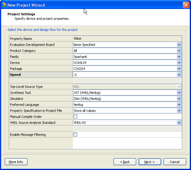
Start Xilinx ISE and select a new project from the File menu. The project wizard will pop up. Type in a project name and path in the first page. Select appropriate FPGA device in the second page. Mimas V2 has a Spartan 6 LX9 device (XC6SLX9). Settings, as shown in the image below, should work fine.
Click next and finish the wizard. Surprisingly we are not going to create or add any source files to the project and our use of ISE’s graphical user interface ends once we generate the required IP and other files using Coregen tool. To start Coregen tool, go to the Tools menu and select “Core Generator”.
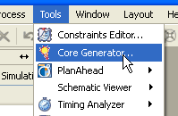
If Core Generator does not create a project automatically, create a project by selecting File>New Project. You will need to select the FPGA and its package when creating the project. Select Verilog as a design entry method. This is to make sure that Core Generator generates code in Verilog. In the IP catalog window, Find MIG under “Memory & Storage Elements” Category.
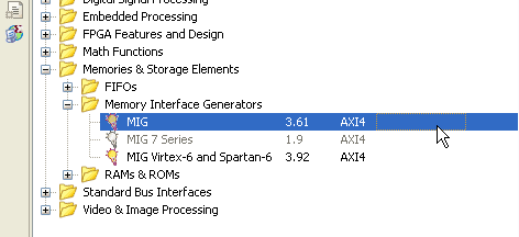
Double click to run Memory Interface Generator wizard. On the first screen, make sure that the selected FPGA device and other settings are correct. The settings should look like in the image below.
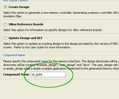
Click next to proceed to the next screen and type in a component name if necessary. Leaving the default name should work fine as well. For the sake of clarity, we will call our component “s6_lpddr”. Please replace this with the component name you chose when “s6_lpddr” appears later in this tutorial.
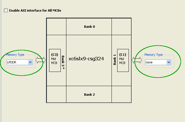
Click next to go to screen three of the wizard. Leave all options unchanged and proceed to screen 4. This screen is where we select the type of DDR memory and tell the MIG wizard where it is connected. Spartan 6 LX9 device has two memory controllers available. On Mimas V2 FPGA Development Board, the LPDDR device is connected to Bank 3 of the FPGA. Select LPDDR from the combo box corresponding to Bank 3. Leave Bank 1 settings unchanged. Settings on this page should look like as in the image below.
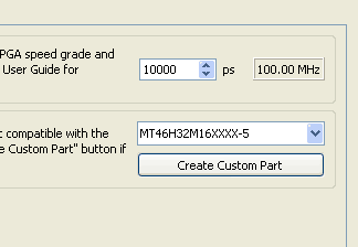
Click next to go to the next screen. This is the place where we select the DDR memory device and its operating frequency. Mimas V2 has onboard LPDDR memory which is Micron MT46H32M16 or equivalent. This device supports DDR clock up to 166MHz. Select MT46H32M16 memory device and set the clock period to 10,000. Clock period 10,000 corresponds to 100MHz DDR clock frequency. Though the DDR device supports up to 166MHz clock, we will use 100MHz to avoid the complication of messing with the PLL settings later. Mimas V2 has a 100MHz clock source and by using the same frequency for DDR clock, we can leave the PLL settings generated by MIG as is. Below is the image with correct memory part and frequency selected.
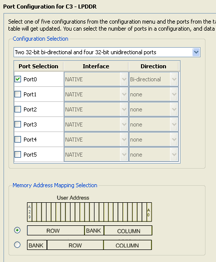
Click next to proceed to the next screen and leave all settings to its defaults. Click next again to proceed to the port configuration screen. Select Port 0 and leave rest of the ports unchecked as shown below.
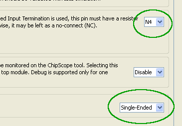
Click next to proceed to the arbitration configuration page. Since we are using only one port, there are no parameters to change on this screen. Click next again to proceed to FPGA Options screen. Select N4 as RZQ pin location and select Single Ended as system clock input. See image below with correct settings.
Click the next button a few more times and finish. Core Generator will generate a bunch of files. These files can be found under the directory \ipcore_dir\s6_lpddr (Assuming you used the name “s6_lpddr” for the auto-generated component). You will see three folders here, docs, example_design and user_design. docs folder has some very important documentation that can be used to learn more about Spartan 6 Memory Controller and the IP generated by MIG. Keep them for a later read.
Editing user constraints
Right now we are going to use the example design generated by MIG. The example design can be found (unsurprisingly) under the folder example_design. There are a few folders and files inside the example_design folder. rtl folder has all the Verilog files generated by MIG. par folder contains some batch files and scripts to build the example design. The user constraints seem to be auto-generated to match with Xilinx’s own development boards. Some changes are necessary to make the auto-generated code work with Mimas V2. Before building the project, we need to do the following.
- Edit the ucf file to make it usable with Mimas V2
- Configure the build environment to generate a binary configuration file
Go to par folder and find example_top.ucf. Open example_top.ucf using any text editor of your choice. Make the following changes.
- Change the line CONFIG VCCAUX=2.5; to CONFIG VCCAUX=3.3; . This change is necessary because Mimas V2 uses 3.3V for VCCAUX.
- Change the following lines
NET “error” IOSTANDARD = LVCMOS18;
NET “calib_done” IOSTANDARD = LVCMOS18;
NET “calib_done” LOC = “B2” ;
NET “error” LOC = “A2” ;ToNET “error” IOSTANDARD = LVCMOS33;
NET “calib_done” IOSTANDARD = LVCMOS33;
NET “calib_done” LOC = “T18” ; #LED1
NET “error” LOC = “T17” ; #LED2
Above changes will make the “error” and “calib_done” pins operate at LVCMOS33 IO standard and assign the nets to T18 and T17 of FPGA where LED1 and LED2 are connected. This will cause LED1 to turn on when calibration is done and LED2 to turn on if memory test failed
- Change the linesNET “c3_sys_clk” IOSTANDARD = LVCMOS25;
NET “c3_sys_rst_n” IOSTANDARD = LVCMOS18;ToNET “c3_sys_clk” IOSTANDARD = LVCMOS33;
NET “c3_sys_rst_n” IOSTANDARD = LVCMOS33;
Above change will set the IO standards for clock input and reset input to LVCMOS33. This is again because the bank that these IO belongs is powered by 3.3V rail.
- Add a line NET “c3_sys_rst_n” PULLDOWN;
This will enable pull down on the reset pin and will keep the memory controller our of reset without having to use any external components. Despite the name “c3_sys_rst_n”, MIG seems to be configuring reset input as active high.
- Change “c3_sys_clk” and “c3_sys_rst_n” pin assignments as below.
NET “c3_sys_clk” LOC = “V10” ;
NET “c3_sys_rst_n” LOC = “M16” ;
This will assign correct IO pads for clock input and assign switch SW3 as reset input.
We are done with the changes in ucf file now. This may seem difficult but easy enough if done carefully. It is a good idea to back up your original ucf file before saving the changes just in case if you want to go back and restart again.
Building the code
Next step is to modify the build environment to generate a binary configuration file. This is a very easy step to do. Find the file mem_interface_top.ut and open it in a text editor. Find the line “-g Binary:no” and change it to “-g Binary:yes” and save.
Now we are ready to build the project. Before building the project, make sure that the path to Xilinx build tools is added to PATH environment variable. Usually, the path is C:\Xilinx\\ISE_DS\ISE\bin\nt assuming ISE is installed on C: drive.
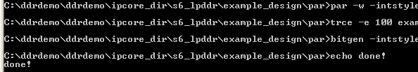
Now run the batch file ise_flow.bat by double-clicking the file or by using the command prompt. If everything went fine so far, the batch file will run the necessary tools to build the project and you will end up with a “Done” message and a bunch of new files in the par folder. The message should look like in the image below.
If the build process fails, refer to ise_flow_results.txt for more details on the causes of failure. You should see the file “example_top.bin” in par folder if build succeeded. This is the file we are going to program Mimas V2 Spartan 6 FPGA development board with.
Configuring Mimas V2 and testing
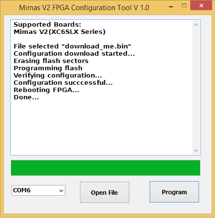
Programming Mimas V2 Spartan 6 FPGA development board is very easy. Download the latest version of the Configuration Downloader Application from the product page. Run the executable, no installation required. Load the binary file and program the flash as illustrated in the image below.
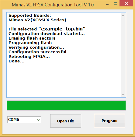
Watch the log window and confirm the configuration binary file is downloaded successfully. Now we are ready to test if the memory interface is working.
Testing if the example program we built, is very easy to do. You may remember we changed a few lines in the ucf file. Below are two of those lines.
NET “calib_done” LOC = “T18” ; #LED1
NET “error” LOC = “T17” ; #LED2
The first line assigns the FPGA pin T18 to the net “calib_done” net and the second line assigns FPGA pin T17 to “error” net. These FPGA pins are connected to LED1 and LED2 respectively. To verify proper functioning of the example program, all that we need to do is to check and make sure that LED connected to “calib_done” (LED1) turns on after power-up, indicating successful completion of initial calibration and the LED connected to “error” (LED2) stays off.
If you have observed calib_done going high and error stays low for a while, congratulations, you’ve got your Spartan 6 DDR SDRAM test project working. Thanks to Xilinx Memory Interface Generator for generating complete and ready to go code.
Creating, configuring and building memory controller core and test program on Xilinx EDK
It is quite easy to generate and build a simple sample program that can test the DDR SDRAM using ISE and it certainly is exciting. It would be more exciting if we could test the whole memory and print the output through UART. Yes, it is possible to do that using Xilinx EDK. And also you could write simple C code to access the DDR SDRAM. We will show you how!
You will need the following tools to implement this project.
- Xilinx EDK (More info here)
- Mimas V2 FPGA Development Board
- A USB Cable
- Mimas V2 Configuration Tool (Download from the product page)
What is Microblaze?
Microblaze is a 32-bit soft processor IP that is developed by Xilinx for their mid – high-end FPGA devices. Microblaze is compatible with their Spartan 6, Virtex and Zynq devices. You can find more resources including datasheet for Microblaze at Xilinx’s Microblaze page. Fortunately, we do not need to download Microblaze IP separate since it is bundled with Xilinx EDK tool. Microblaze based embedded design can use either PLB or AXI as the bus system. Since Xilinx is planning to phase out PLB and keep only AXI in the future, we will stick With AXI for our designs. You do not need deep knowledge of Microblaze or AXI to follow this article and build a working system successfully.
What is AXI?
AXI stands for Advanced eXtensible Interface. AXI is a bus interconnect based on ARM’s popular AMBA bus architecture. In a Microblaze based embedded system, AXI connects the microprocessor to all available peripherals. The only exception is Block RAM which is attached to the processor through LMB (Local Memory Bus). AXILite is available for connecting low throughput peripherals to the system such as UART, GPIO etc… AXILite uses fewer logic resources on FPGA compared to AXI. Usually, AXI is used to connect high throughput peripherals such as DDR memory, Ethernet etc.. Again, a detailed understanding of AXI is not required for following this article. But for the curious readers, AXI Reference Guide is available here.
What is EDK?
EDK is a set of development tools provided by Xilinx to help create Microblaze based embedded system and develop software for the system. Xilinx EDK has two main components.
Xilinx Platform Studio (XPS)
Xilinx Software Development Kit (SDK)
These are the two separate software tools that we will use to design and implement our system. XPS is the tool used for designing and generating the hardware system. You will create and configure Microblaze processor and necessary peripherals using XPS and generate a bit file from the design. This bit file will be programmed to the FPGA to complete the hardware design. SDK is the tool where the software is written for the Microblaze processor. The software can be written using C or C++. SDK and XPS together will generate all necessary header files and linker scripts needed to successfully build the software for your system. We will take a detailed look at these tools as we go forward. More details about these tools can be found here.
Creating Microblaze Based Embedded Hardware Platform
In this section, we will see how to create a basic Embedded Platform based on Microblaze using Xilinx Platform Studio (XPS). We will use the base System Builder (BSB) wizard to generate the system. To use BSB to generate a system for Mimas V2, you will need to download the BSB System Wizard files from the product page and extract to the folder “C:\Xilinx\xx.xx\ISE_DS\EDK\board”. Once extracted, the complete path to the file should look like “C:\Xilinx\xx.xx\ISE_DS\EDK\board\NumatoLab\ipxact\MimasV2\data”. Once files extracted properly, go to All Programs > Xilinx Design Tools > EDK and click on Xilinx Platform Studio icon. Once XPS is loaded, click on “New BSB Project” under File menu or press Ctrl + Shift + B to invoke the BSB wizard. If everything went fine, the BSB wizard window will pop up as shown below.
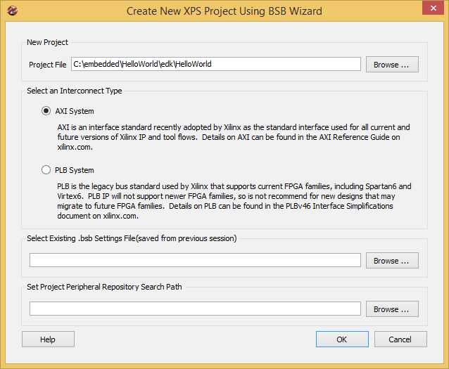
Enter the path to a folder where you want to store the project and type in a project name. Select AXI System in the “Interconnect Type” section and click OK. In the next page of the wizard, select “Numato Lab” from the board Vendor combo box (This option should be available if you have placed the BSB wizard support files for Mimas V2 correctly as mentioned earlier). Select Mimas and 2.0 from Board Name and Board version combo boxes respectively and click the “Next” button.
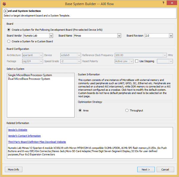
You can set the Optimization strategy to Area or Throughput. We will leave it at the default option “Area” for this example. Click Next to proceed to the next page of the wizard. In the next page, you will have an option to select peripherals as shown in the image below.
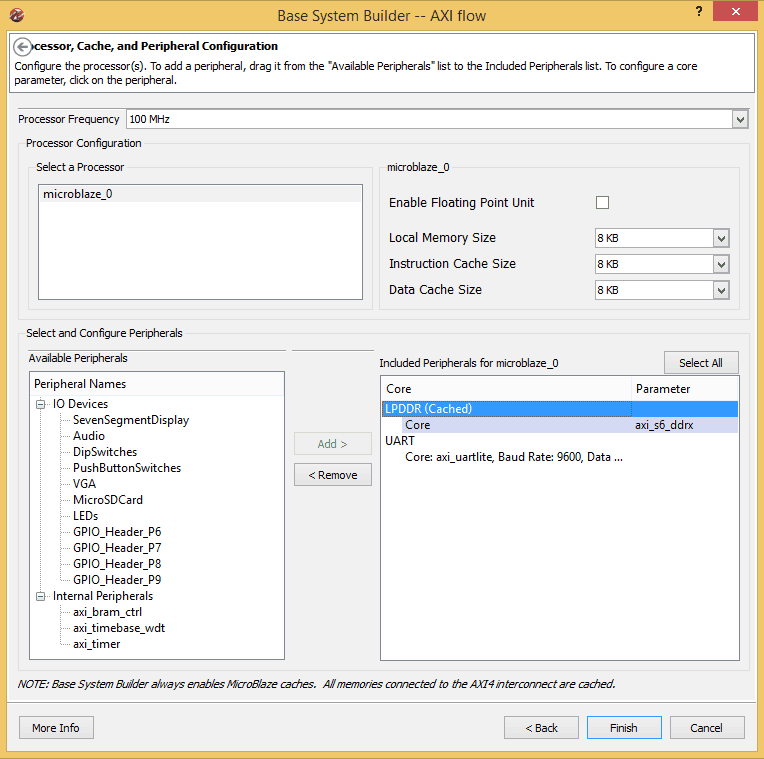
Leave everything in this page to its defaults and click Finish. At this point, XPS will generate the system for you and you will be presented with a window like below.
This window shows all IPs available, IPs used in the design and bus connections between the IPs used. Here you may notice that DDR memory is connected to the Microblaze processor through AXI bus since DDR requires better throughput. But all other peripherals are connected to AXI Lite. To make this system work with Mimas V2 there is certain customization we need to do.
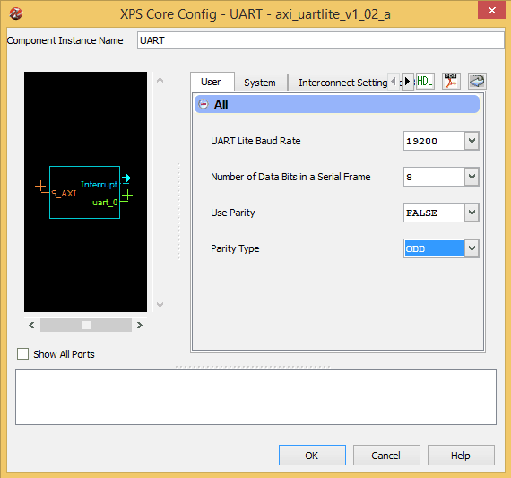
Change baud rate
The first change we need to make is the UART baud rate. Right click on the UART IP in the “Bus Interfaces” view and select “Configure IP”. In the IP configuration window that pops up, select baud rate “19200” and leave all other settings to defaults. Please see the image below to exact settings.
Connect RESET to an external switch
Next thing we need to do is to assign a switch to the “RESET” net of the Microblaze processor so we can reset the whole system when necessary. To do this, open the file “ddrdemo.ucf” file in the project view and replace the line
NET “RESET” PULLUP;
with
NET “RESET” LOC = M16 | IOSTANDARD = LVCMOS33 | DRIVE = 8 | SLEW = FAST | PULLUP;
This will connect the momentary switch SW3 on Mimas V2 to the Processor’s RESET line. This will allow us to reset the processor anytime by pressing switch SW3.
Select CCLK as configuration clock
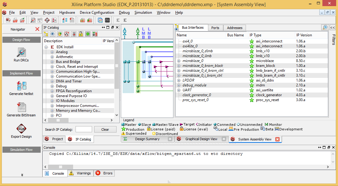
By default, XPS will set JTAG clock as FPGA startup clock. This is perfectly fine if we are using a JTAG adapter such as Xilinx Platform Cable – USB for programming the FPGA. But to use Mimas V2 Configuration utility, we need to set startup clock to CCLK instead of JTAGCLK. To do this, go to the “Project” tab right next to the “IP Catalog” tab in XPS and open the Bitgen Options file “etc/bitgen.ut”. Change the line “-g StartUpClk:JTAGCLK” to “-g StartUpClk:CCLK”. Save the file click on the “Generate Bitstream” button on the left to compile the system and build the bitstream. This step may take a few minutes to a few tens of minutes depending on the speed of your computer.
Once the bit file is generated successfully, click on the “Export Design” button on the toolbar on the left. Click on the “Export Only” button on the window that pops up. This step will export all necessary files for creating an SDK project into a convenient directory (usually inside SDK\SDK_Export\hw under the current project directory). At this point, we have the hardware system ready. This is more or less equivalent to having a microprocessor/microcontroller board without and code written for it. So our next step is to write some code and build it.
Creating an Application program for Microblaze
We will use Xilinx SDK to write and compile code for the hardware platform we just built. Xilinx SDK is an Eclipse-based IDE that can create, build, debug and maintain projects for Xilinx Microblaze based platforms. To start SDK, go to All Programs > Xilinx Design Tools > EDK and select “Xilinx Software Development Kit”. When asked to choose a workspace, enter a convenient directory where you would like the projects files to be stored. To create a new SDK project, select “New Application Project” from File menu. You will be presented with a window like shown below.
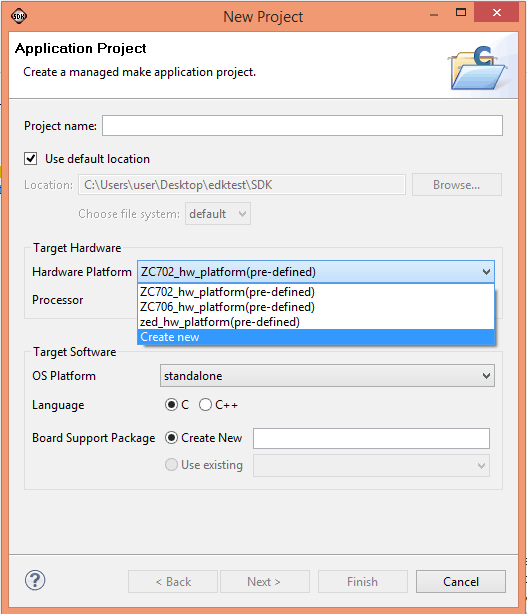
Select create new from the Hardware Platform combo box. A new window will appear where we need to create a new Hardware Project.
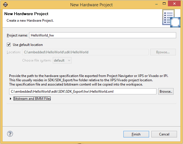
Click on the Browse button and browse to the directory where the XPS project was saved earlier. And browse to SDK\SDK_Export\hw and select ddrdemo.xml. This wizard will automatically populate a project name, we will leave it unchanged. Click Finish button to go back to the Application Project Wizard. Back in the application project wizard, enter a project name and leave all other settings to defaults as shown in the image below.
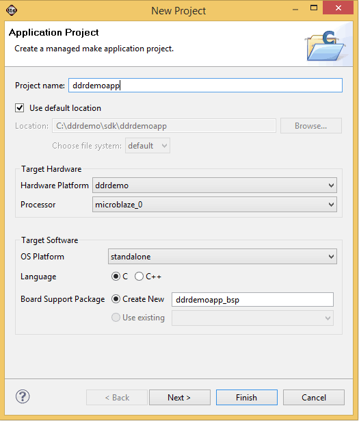
Click next to go to the last page in the application project Wizard. Select “Memory Test” template from the list of templates and click Finish. SDK will create a workspace and add three projects to it. All projects can be viewed in Eclipse Project Explorer as below.
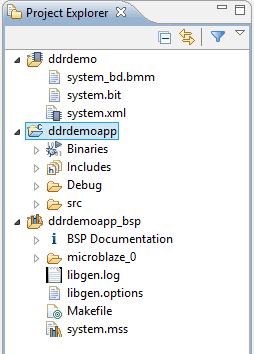
In the image below, you can see three projects. Project on the top is the hardware platform. These files are copied directly from the directory where XPS exported the hardware system to. The one below is the application project that we will be working on. And the one all the way to the bottom is the BSP project which was automatically generated by SDK. The libraries and include files necessary for our application to work are stored under this project.
To build the project, select “Build All” from Project menu. If everything went fine so far, the project should build with no errors. Again this is a working project which can be downloaded and tested on hardware without any modifications. If you would like to see the code, go to src folder under the ddrdemoapp project and open the source files listed there. memorytest.c has the main() function.
Building And Testing The Program
Once the project is successfully created, SDK will build the program on its own. You can force another build by selecting “Build All” from the “Project” menu or pressing Ctrl+B.
Now that we have created and built the projects on XPS and SDK, we can create the final binary image. The idea is to use Xilinx data2mem tool to merge the FPGA bit file generated by XPS for Microblaze system and the executable generated by SDK.
We need to find the following files from the XPS and SDK projects that we have built.
- The bit file (The file name should be ddrdemo.bit if you used the same project name as mine. This file is located in the folder SDK\SDK_Export\hw inside the XPS project folder)
- The executable file (The file name should be ddrdemoapp.elf if you used the same project name as mine. This file is located in the folder ddrdemoapp\Debug inside the SDK workspace folder)
- The .bmm file (The file name should be ddrdemo_bd.bmm if you used the same project name as mine. This file is located in the folder SDK\SDK_Export\hw inside the XPS project folder)
Once all these three files are copied to a common folder, open command line prompt and move to that folder. Follow the two steps below to generate the final bin file.
Step 1
cmd> c:\Xilinx\xx.x\ISE_DS\settings64.bat
cmd> data2mem -bm ddrdemo_bd.bmm -bd ddrdemoapp.elf -bt ddrdemo.bit
Make sure to replace xx.x in the first command with your ISE version to form a correct path and use correct file names in the second command (if your XPS/SDK project names were different). If the commands did run successfully, you should see a new bit file generated in the folder (ddrdemo_rp.bit in my case).
Step 2
Now we need to generate a bin file. Run the following command in the same command window.
cmd> promgen -w -p bin -u 0x0 ddrdemo_rp.bit -spi -o download_me
If the command was successful, you will see a few new files generated in the folder. One of the files will be download_me.bin. We will use this file to configure Mimas V2. Run Mimas V2 flash configuration tool (make sure to set the slider switch on Mimas V2 into programming mode, please see details in the user manual), select download_me.bin and click “program” button as in the image below.
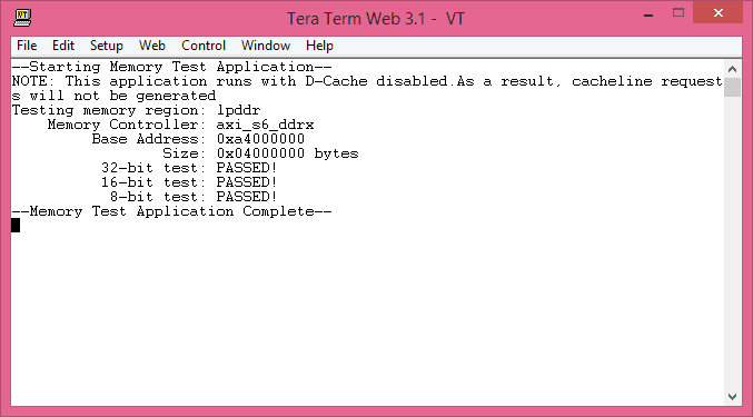
Once the board is programmed, put the slider switch on Mimas V2 into normal mode and connect to the COM port corresponding to the board using any serial terminal emulation software such as Hyperterminal or TeraTerm. Then press the switch SW3 to reset the processor. If everything went well so far, you should see the following test results printed on the terminal.
This tutorials shows how easy it is to generate and build simple test applications to exercise the DDR SDRAM available on Mimas V2 FPGA Development Board (or any other Spartan 6 based board for that matter).
Back to part 5
I used the ISE Core Generator (MIG) to create the bin file for programming the fpga. I walked through the steps 4 different times to make sure I was understanding and following the procedure. The final result was MIG never generated the final files, nor did it give me any faults. The ise_flow_results.txt file had nothing in it either. This was the only file the ise_flow.bat file made. I would really appreciate it if someone had some suggestions for me to try.
May 3, 2016 at 3:10 pmThanks.
Hi Jeff, I can only guess but most probably the problem would be with the ISE installation. Is there a way to try the steps on a different machine or at least re-install ISE on the same machine ? As far as the steps go, they are tested on ISE14.4 many dozens of times. So that shouldn’t be a problem. Another useful thing to try is to generate core with some other configuration, just to make sure the problem is only with this particular configuration mentioned in this tutorial.
Thanks
May 5, 2016 at 5:49 pmhey you’ve got to run : “D:ISE_Design_Studio14.7ISE_DSsettings64.bat” or “D:ISE_Design_Studio14.7ISE_DSsettings32.bat” depending on whether your system has 32/64 bit cpu + windows. Run it in a command window, then in the same command window run the ise_flow.bat
June 14, 2016 at 3:08 pmI followed the steps to change the UCF file and tried to compile with errors
Phase 2.7 Design Feasibility Check
INFO:Place:834 – Only a subset of IOs are locked. Out of 179 IOs, 44 are locked
and 135 are not locked. If you would like to print the names of these IOs,
please set the environment variable XIL_PAR_DESIGN_CHECK_VERBOSE to 1.
ERROR:Place:1205 – This design contains a global buffer instance,
, driving the net, ,
that is driving the following (first 30) non-clock load pins off chip.
also “c3_sys_rst_n” did not exists in the UCF fie, although “c3_sys_rst_i” existed, so I just renamed “c3_sys_rst_n” to “c3_sys_rst_i” but no luck.
June 14, 2016 at 2:32 pmI noticed these were also in another UCF file , i.e. s6_lpddr.ucf , maybe I’m not compiling the correct top module? However the names “c3_sys_rst_n” still don’t exist, it’s “c3_sys_rst_i” in mine
June 14, 2016 at 2:41 pmokay so I ran ISE_Design_Studio14.7ISE_DSsettings64.bat in command window , then “ipcore_direxample_designparcreate_ise.bat” and it made “test.xise” and loaded it with ISE Design Studio. Now I’m able to compile and run it. The board just has D8 LED continuously on (T18) so I guess calib is done, but when I press SW3 I see no sign of it trying to reset…. anyway
June 14, 2016 at 3:23 pmIt is a good starting documentation for newbies like me
August 11, 2017 at 4:18 pmThanks for the time and effort to put things together
Where can i take tutorial source code files?
December 17, 2018 at 2:56 am