Introduction
Learning electronics can be a bit challenging sometimes, but it is really fun if you have a little patience to read, understand, and experiment. FPGAs need not be any different. Let us give it a try and see how fast and easily we can learn a little bit about FPGAs and create a simple working test project with this easy FPGA tutorial. To get the best out of this tutorial series, I strongly recommend downloading the tools listed at the end of this document and try doing every step as you read along.
Some time back, I wanted to learn about programming FPGAs. I started googling only to find that there is no FPGA tutorial on the web (that is the case when this tutorial was originally written. But there should be more FPGA tutorials available online now!) that can get you started with learning a little bit of HDL and take you all the way through design, simulation, and implementation. There are many tutorials online that will help you learn HDLs, some tutorials tell you how to do simulation, some may tell you about implementation, but no single tutorial that guides you step by step from basics to implementation.
I decided to write this tutorial in the hope that it may help our readers to learn a little bit of Verilog (The HDL I chose to learn first because of its syntax similarity to C), simulate your code and implement it on real hardware. This tutorial expects you to have basic knowledge in Digital Electronics, Familiarity with some programming language (preferably C). This tutorial is not meant to be an in-depth study about Verilog or FPGAs or anything, but just a guide to walk you through different basic things you need to know to design a simple digital circuit in Verilog, simulate it and implement it on hardware.
We will be using Xilinx ISE for simulation and synthesis. ISE Webpack version 14.7 is preferred, which is the latest version available (and last since Xilinx moved on to Vivado). If asked during installation, install “System Edition” because it will include Xilinx EDK as well. Please note that ISE Webpack and EDK licenses are separate. You will need ISE license installed to follow the next few parts of this tutorial. Please note that EDK evaluation license is only valid for 30 days but ISE Webpack license is perpetual. The final design will be programmed to an Elbert – Spartan 3A FPGA Development Board to make sure our code works on real hardware as well.
You can also follow along with an alternative version of this guide using a Mimas A7 – Artix 7 FPGA Board on the following link.
What is FPGA?
FPGA stands for “Field Programmable Gate Array“. As you may already know, FPGA essentially is a huge array of gates that can be programmed and reconfigured any time anywhere. “Huge array of gates” is an oversimplified description of FPGA. FPGA is indeed much more complex than a simple array of gates. Some FPGAs have built-in hard blocks such as Memory controllers, high-speed communication interfaces, PCIe Endpoints, etc. But the point is, there are a lot of gates inside the FPGA which can be arbitrarily connected together to make a circuit of your choice. More or less like connecting individual logic gate ICs (again oversimplified but a good mental picture nonetheless). FPGAs are manufactured by companies like Xilinx, Altera, Microsemi, etc… FPGAs are fundamentally similar to CPLDs but CPLDs are very small in size and capability compared to FPGAs.
What are the applications of FPGA?
Architecturally FPGAs are essentially a sea of gates that can be reconfigured to build almost any digital circuit that one can imagine. This great flexibility along with the ability to reconfigure the device with different designs at-will makes FPGA a better choice compared to ASICs (Application Specific Integrated Circuit) for a lot of applications. For example, deep learning, AI, or application acceleration system can re-program a single FPGA with different algorithms at different times to achieve the best performance. An ASIC would not be as flexible in such situations. In certain applications, the number of individual units manufactured would be very small. Designing and manufacturing ASICs for these applications can be prohibitively expensive. In such situations, FPGA can offer very cost-effective but robust solutions. The module form-factor boards such as the Narvi Spartan 7 FPGA Module make it easier to implement the applications without requiring end-product designers to take care of complex details such as FPGA power supplies, DDR3 routing, etc. Below are some of the potential applications of FPGAs in no particular order.
- Cryptography
- ASIC prototyping
- Industrial, medical and Scientific Instruments
- Audio/Video and Image processing and broadcasting
- High-performance computing, AI, and Deep Learning
- Military and Space applications
- Networking, packet processing, and other communications
What is FPGA programming?
FPGA programming or FPGA development process is the process of planning, designing, and implementing a solution on FPGA. The amount and type of planning vary from application to application. But creating a requirements document that captures all specific requirements and creating a design document that explains how the proposed solution would be implemented can be very helpful to enumerate potential problems and plan around them. A little bit of time spent creating a quality design document will save tons of time in refactoring, debugging, and bug fixing later. Implementing a solution on FPGA includes building the design using one of the design entry methods such as schematics or HDL code such as Verilog or VHDL, Synthesizing the design (Synthesis, netlist generation, place, and route, etc.) into output files that FPGAs can understand and program the output file to the physical FPGA device using programming tools. Entering the design using schematics is not used in the industry widely anymore. So we will keep the discussion limited to design entry using HDL (Hardware Description Language), specifically Verilog in this article series. Synthesis and programming are almost completely taken care of the vendor tools such as ISE and Vivado and Numato Lab configuration tools. All necessary steps to be taken by the user as part of design entry, synthesis and programming will be explained in subsequent sections.
What is RTL?
RTL stands for Register Transfer Level. You might also encounter the terms Register Transfer Logic or Register Transfer Language, they all mean the same in the context of hardware designing. RTL is a higher-level abstraction for your digital hardware design and comes somewhere between strictly behavioral modeling on one end and purely gate-level structural modeling on other ends. Behavioral modeling is explained in the next articles in this series so don’t be daunted with this term. Gate modeling means describing hardware using basic gates which is quite tedious. RTL can also be thought of as analogous to the term “pseudo-code” used in software programming. It is possible to describe the hardware design as sequences of steps (or flow) of data from one set of registers to next at each clock cycle. Therefore, RTL is also commonly referred to as “dataflow” design. Once the RTL design is ready, it is easier to convert it into actual HDL code using languages such as Verilog, VHDL, SystemVerilog, or any other hardware description language. HDL and Verilog are explained in the next section. Check out the Wikipedia page on RTL for more information (https://en.wikipedia.org/wiki/Register-transfer_level)
What is Verilog?
In the previous paragraphs, I mentioned the word “oversimplified” two times. The reason is that FPGAs are much much more than just a bunch of gates. While it is possible to build logic circuits of any complexity simply by arranging and connecting logic gates, it is just not practical and efficient. So we need a way to express the logic in some easy to use format that can be converted to an array of gates eventually. Two popular ways to accomplish this are schematic entry and HDLs (Hardware Description Language). Before HDLs were popular, engineers used to design everything with schematics. Schematics are wonderfully easy for small designs but are painfully unmanageable for a large design (think about Intel engineers drawing schematics for Pentium, which has millions of gates! it is unacceptably complex). If you have some electronics background, your initial tendency will be to use schematics to realize your design instead of learning a new language (This happened to me, honestly). For the aforementioned reasons, we will stick with HDL throughout this tutorial.
Verilog is a Hardware Description Language (HDL) which can be used to describe digital circuits in a textual manner. We will write our design for FPGA using Verilog (as if you write microcontroller programs in C and Assembly). Learning Verilog is not that hard if you have some programming background. VHDL is also another popular HDL used in the industry extensively. Verilog and VHDL share more or less same market popularity, but I chose Verilog since it is easy to learn and its syntactical similarity to C language. Once you are comfortable with Verilog, it should be easy to learn VHDL as well. Want to read more about Verilog? Check out this wiki page (http://en.wikipedia.org/wiki/Verilog) or check this tutorial (http://www.asic-world.com/verilog/index.html).
What tools do we need?
1. A good text editor (I use Notepad++ )
2. Xilinx ISE Webpack (Download from Xilinx for free. Registration required).
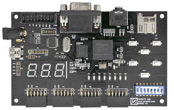
3. A good FPGA development board (Mimas V2 FPGA Development Board is used in the examples here. The picture of Mimas V2 is shown at the top of this page. If you have an Elbert V2 Spartan 3A FPGA board, that should work perfectly too. There are some differences when setting up the project for Mimas V2 vs Elbert V2 but I will point them out when it is necessary.)
4. Mimas V2 or Elbert V2 Configuration downloader software (Required only if Mimas V2 /Elbert V2 FPGA Development Board is used. Download from the respective product pages)
Additional tools may be necessary to follow advanced topics in this series. Information about such tools will be shared as they are needed.
Continue to part 2
It is really helpful to me Because I understand all procedure
June 15, 2016 at 7:38 amit links me to vivado we installer, is it good?
July 28, 2016 at 10:06 amLook for ISE tab on the page. Vivado is the default tab but just one of the many tabs available.
August 4, 2016 at 2:59 pmis that we can say an FPGA is simillar to a breadboard withcircuitary connected.
February 4, 2017 at 1:39 amVGuru for Verilog and VHDL is very good software for beginners, to learn with all the best practice. I have used and learnt all the concepts. https://youtu.be/K9R3CYOlCiM
February 5, 2017 at 3:22 amHi, if it is possible a to ask a suggestion. I bought a book on amazon “Video Game Engine Development Guide (Using Xilinx SoC Board)”. It refer to a Spartan 3E-1600 MicroBlaze Development Board. It seems difficult to find and very expensive and i am wondering if there is something similar (and cheaper) or I must use that exact board. Thanks for the help
October 25, 2017 at 10:32 pmHi,
October 27, 2017 at 9:08 pmCan ISE be installed and run on windows 10. I remember I had problems running ISE 6 months ago. Thanks.
I bought a Vivado compatible board would that work with your beginners intro?
Theres a company in USA In Washington that supports Xilinx sells these boards I forget it’s name.
Could I use any other FPGA Software I also have Altera!?
In Altera CPLD version it supports older gates but those gates are abbreviated I have no clue what they are,
would anbody know anything about that (I’m a newbie you know).
Can the designer use a block diagram for projects, to do this would I need to include all gates in just one block
Diagram?
I was always baffled in how to figure out the pin arrangement for each gate?
Anyways I will experiment away?
March 23, 2019 at 2:01 amMany thanks sorry for my large comment. 🙂