

1.Introduction
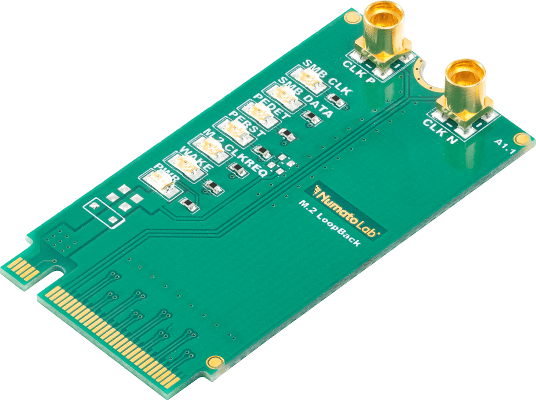
The M.2 loopback module, enables signal integrity testing of PCIe lanes in custom M.2 host board designs. It features a high-frequency PCB with controlled-impedance routing that loops back all four PCI Express lanes for validation and testing purposes. The module supports PCIe Gen3 data rates up to 8 GHz.
 Was this helpful?
2.Applications
- PCIe Gen1/Ge2/Gen3/Gen4 loopback testing
- FPGA PCIe transceiver/GT loopback testing
- IBERT and PRBS/BER testing
- Testing all four PCIe lanes
- High-speed signal integrity and PCB validation
- PCIe link bring-up and debugging
3.Features
-
Compatible with M.2 M-Key connectors used for PCIe SSD interfaces
-
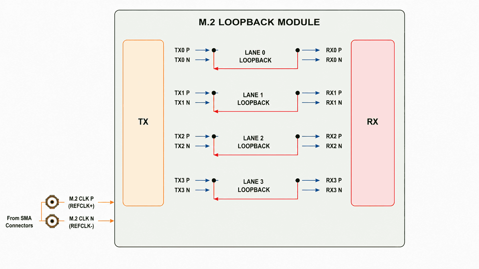
Supports loopback testing for all four PCIe lanes
-
Supports PCIe Gen1, Gen2, and Gen3 operation (2.5 GT/s to 8 GT/s)
-
MMCX connectors are provided for external differential clock input through the CLK_P and CLK_N signals
-
LEDs for status indication
4.Functional Block Diagram
6.Connection Diagram
7.Connection Details
| SL.No | Signal Details | Pin Location | ||
|---|---|---|---|---|
| 1 | M.2_CLK_P | REFCLKp | ||
| 2 | M.2_CLK_N | REFCLKn | ||
| 3 | M.2_RX0_P | PETp0 | ||
| 4 | M.2_RX0_N | PETn0 | ||
| 5 | M.2_TX_0_P | PERp0 | ||
| 6 | M.2_TX_0_N | PERn0 | ||
| 7 | M.2_RX1_P | PETp1 | ||
| 8 | M.2_RX1_N | PETn1 | ||
| 9 | M.2_TX_1_P | PERp1 | ||
| 10 | M.2_RX2_P | PETp2 | ||
| 11 | M.2_RX2_N | PETn2 | ||
| 12 | M.2_TX_2_P | PERp2 | ||
| 13 | M.2_TX_2_N | PERn2 | ||
| 14 | M.2_RX3_P | PETp3 | ||
| 15 | M.2_RX3_N | PETn3 | ||
| 16 | M.2_TX_3_P | PERp3 | ||
| 17 | M.2_TX_3_N | PERn3 | ||
| 18 | SMB_DATA | SMB_DATA | ||
| 19 | SMB_CLK | SMB_CLK |
8.Technical Specification
| Parameter | Value | Unit |
|---|---|---|
| Basic Specifications | ||
| Form Factor | 2242 | mm |
| M.2 Key Type | M-Key | |
| PCIe Lanes | 4 (x4) | Lanes |
| PCIe Generation | Gen1 / Gen2 / Gen3/Gen4 | |
| PCIe Data Rate | 2.5 / 5 / 8 | GT/s |
| Module Supply | 3.3 | V |
| Status LEDs | Power / WAKE# / SMBus / PERST# |
9.Mechanical Dimensions
Help Guide Powered by Documentor