

1.Introduction
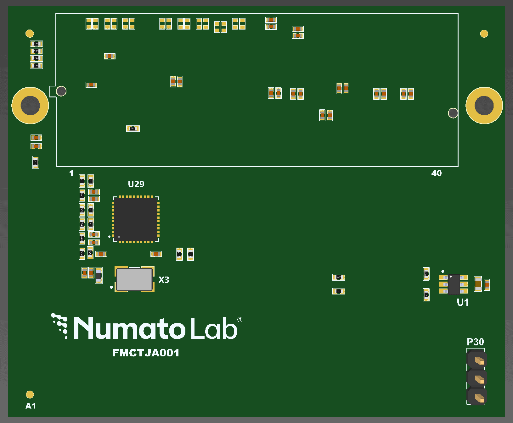
The Numato Lab FMC HPC Loopback Module is designed for testing and validating high-speed signal connectivity between an FMC-compatible FPGA carrier board and the module. The module provides direct loopback paths for the FMC interface signals, enabling convenient testing of FPGA I/O and high-speed transceiver interfaces without requiring external signal connections.
The module is compliant with the ANSI/VITA 57.1 FMC standard and uses an FMC HPC connector to provide access to the available LA, HA, HB, and high-speed transceiver signals. It supports 34 LA differential pairs, 24 HA differential pairs, 22 HB differential pairs, and up to 10 high-speed transceiver pairs. The HPC interface therefore provides up to 80 user-defined differential I/O pairs in addition to the high-speed transceiver interfaces.
An on-board programmable Si5332A-GM2 clock generator provides up to eight clock outputs, with a default frequency of 100 MHz on all outputs. An I2C EEPROM is also provided on the module for storing configuration information.
 Was this helpful?
1.1.Applications
- FPGA I/O and interface validation
- High-speed signal loopback testing
- FMC HPC interface connectivity testing
- Hardware debugging and troubleshooting
1.2.Board Features
- FMC HPC interface compliant with the ANSI/VITA 57.1 FMC Standard
- ASP-184330-01 FMC HPC connector
- On-board I2C EEPROM for configuration storage
- Supports:
- LA (34 differential pairs)
- HA (24 differential pairs)
- HB (22 differential pairs)
- High-speed transceiver DP signals (10 differential pairs.
- Compact 69 mm × 57 mm form factor
- Programmable Si5332A-GM2 clock generator available on board
- Default frequency: 100 MHz on all 8 clock outputs
2.How to use the module
The following section describes how to use this module.
2.1.Compatible FPGA Boards
- Neutron KU60 FPGA Development Board
- TityraCore SoC Carrier
- EagleCore C02
- Nereid k7 PCIe Express FPGA Development Module
- Tagus A7 PCIe Express Development Board
- Proteus K7 USB 3.1 Development Board
Supports All the FPGA boards with a standard FMC HPC connector and pinout.
3.Connection Details
Loopback details of FMC LA Pins
| PIN NAME | SIGNAL NAME |
|---|---|
| G6 <-> H7 | LA00_P_CC <-> LA02_P |
| G7 <-> H8 | LA00_N_CC <-> LA02_N |
| G9 <-> H10 | LA03_P <-> LA04_P |
| G10 <-> H11 | LA03_N <-> LA04_N |
| G12 <-> H13 | LA08_P <-> LA07_P |
| G13 <-> H14 | LA08_N <-> LA07_N |
| G15 <-> H16 | LA12_P <-> LA11_P |
| G16 <-> H17 | LA12_N <-> LA11_N |
| G18 <-> H19 | LA16_P <-> LA15_P |
| G19 <-> H20 | LA16_N <-> LA15_N |
| G21 <-> H22 | LA20_P <-> LA19_P |
| G22 <-> H23 | LA20_N <-> LA19_N |
| G24 <-> H25 | LA22_P <-> LA21_P |
| G25 <-> H26 | LA22_N <-> LA21_N |
| G27 <-> H28 | LA25_P <-> LA24_P |
| G28 <-> H29 | LA25_N <-> LA24_N |
| G30 <-> H31 | LA29_P <-> LA28_P |
| G31 <-> H32 | LA29_N <-> LA28_N |
| G33 <-> H34 | LA31_P <-> LA30_P |
| G34 <-> H35 | LA31_N <-> LA30_N |
| G36 <-> H37 | LA33_P <-> LA32_P |
| G37 <-> H38 | LA33_N <-> LA32_N |
| C9 <-> D10 | LA06_P <-> LA05_P |
| C10 <-> D11 | LA06_N <-> LA05_N |
| C13 <-> D14 | LA10_P <-> LA09_P |
| C14 <-> D15 | LA10_N <-> LA09_N |
| C17 <-> D18 | LA14_P <-> LA13_P |
| C18 <-> D19 | LA14_N <-> LA13_N |
| C21 <-> D22 | LA18_P <-> LA17_P_CC |
| C22 <-> D23 | LA18_N <-> LA17_N_CC |
| C25 <-> D26 | LA27_P <-> LA26_P |
| C26 <-> D27 | LA27_N <-> LA26_N |
Loopback details of FMC HA Pins
| PIN NAME | SIGNAL NAME |
|---|---|
| E2 <-> F4 | HA01_P_CC <-> HA00_P_CC |
| E3 <-> F5 | HA01_N_CC <-> HA00_N_CC |
| E6 <-> F7 | HA05_P <-> HA04_P |
| E7 <-> F8 | HA05_N <-> HA04_N |
| E9 <-> F10 | HA09_P <-> HA08_P |
| E10 <-> F11 | HA09_N <-> HA08_N |
| E12 <-> F13 | HA13_P <-> HA12_P |
| E13 <-> F14 | HA13_N <-> HA12_N |
| E15 <-> F16 | HA16_P <-> HA15_P |
| E16 <-> F17 | HA16_N <-> HA15_N |
| E18 <-> F19 | HA20_P <-> HA19_P |
| E19 <-> F20 | HA20_N <-> HA19_N |
| J6 <-> K7 | HA03_P <-> HA02_P |
| J7 <-> K8 | HA03_N <-> HA02_N |
| J9 <-> K10 | HA07_P <-> HA06_P |
| J10 <-> K11 | HA07_N <-> HA06_N |
| J12 <-> K13 | HA11_P <-> HA10_P |
| J13 <-> K14 | HA11_N <-> HA10_N |
| J15 <-> K16 | HA14_P <-> HA17_P_CC |
| J16 <-> K17 | HA14_N <-> HA17_N_CC |
| J18 <-> K19 | HA18_P <-> HA21_P |
| J19 <-> K20 | HA18_N <-> HA21_N |
| J21 <-> K22 | HA22_P <-> HA23_P |
| J22 <-> K23 | HA22_N <-> HA23_N |
Loopback details of FMC HB Pins
| PIN NAME | SIGNAL NAME |
|---|---|
| E21 <-> F22 | HB03_P <-> HB02_P |
| E22 <-> F23 | HB03_N <-> HB02_N |
| E24 <-> F25 | HB05_P <-> HB04_P |
| E25 <-> F26 | HB05_N <-> HB04_N |
| E27 <-> F28 | HB09_P <-> HB08_P |
| E28 <-> F29 | HB09_N <-> HB08_N |
| E30 <-> F31 | HB13_P <-> HB12_P |
| E31 <-> F32 | HB13_N <-> HB12_N |
| E33 <-> F34 | HB19_P <-> HB16_P |
| E34 <-> F35 | HB19_N <-> HB16_N |
| E36 <-> F37 | HB21_P <-> HB20_P |
| E37 <-> F38 | HB21_N <-> HB20_N |
| J24 <-> K25 | HB01_P <-> HB00_P_CC |
| J25 <-> K26 | HB01_N <-> HB00_N_CC |
| J27 <-> K28 | HB07_P <-> HB06_P_CC |
| J28 <-> K29 | HB07_N <-> HB06_N_CC |
| J30 <-> K31 | HB11_P <-> HB10_P |
| J31 <-> K32 | HB11_N <-> HB10_N |
| J33 <-> K34 | HB15_P <-> HB14_P |
| J34 <-> K35 | HB15_N <-> HB14_N |
| J36 <-> K37 | HB18_P <-> HB17_P_CC |
| J37 <-> K38 | HB18_N <-> HB17_N_CC |
Loopback details of transceiver pins
| PIN NAME | SIGNAL NAME |
|---|---|
| A2 <-> A22 | HSPC_DP1_M2C_P <-> HSPC_DP1_C2M_P |
| A3 <-> A23 | HSPC_DP1_M2C_N <-> HSPC_DP1_C2M_N |
| A6 <-> A26 | HSPC_DP2_M2C_P <-> HSPC_DP2_C2M_P |
| A7 <-> A27 | HSPC_DP2_M2C_N <-> HSPC_DP2_C2M_N |
| A10 <-> A30 | HSPC_DP3_M2C_P <-> HSPC_DP3_C2M_P |
| A11 <-> A31 | HSPC_DP3_M2C_N <-> HSPC_DP3_C2M_N |
| A14 <-> A34 | HSPC_DP4_M2C_P <-> HSPC_DP4_C2M_P |
| A15 <-> A35 | HSPC_DP4_M2C_N <-> HSPC_DP4_C2M_N |
| A18 <-> A38 | HSPC_DP5_M2C_P <-> HSPC_DP5_C2M_P |
| A19 <-> A39 | HSPC_DP5_M2C_N <-> HSPC_DP5_C2M_N |
| B16 <-> B36 | HSPC_DP6_M2C_P <-> HSPC_DP6_C2M_P |
| B17 <-> B37 | HSPC_DP6_M2C_N <-> HSPC_DP6_C2M_N |
| B12 <-> B32 | HSPC_DP7_M2C_P <-> HSPC_DP7_C2M_P |
| B13 <-> B33 | HSPC_DP7_M2C_N <-> HSPC_DP7_C2M_N |
| B8 <-> B28 | HSPC_DP8_M2C_P <-> HSPC_DP8_C2M_P |
| B9 <-> B29 | HSPC_DP8_M2C_N <-> HSPC_DP8_C2M_N |
| B4 <-> B24 | HSPC_DP9_M2C_P <-> HSPC_DP9_C2M_P |
| B5 <-> B25 | HSPC_DP9_M2C_N <-> HSPC_DP9_C2M_N |
4.Technical Specification
| Parameter | Value | Unit |
|---|---|---|
| Basic Specification | ||
| FMC Interface Standard | ANSI/VITA 57.1 FMC | |
| FMC Connector Type | HPC (High Pin Count) | |
| Number of User I/O Differential Pairs | 80 | Pairs |
| LA Differential Pairs | 34 | Pairs |
| HA Differential Pairs | 24 | Pairs |
| HB Differential Pairs | 22 | Pairs |
| High-Speed Transceiver DP Pairs | 10 | Pairs |
| On-board Clock Generator | Si5332A-GM2 | |
| Number of Clock Outputs | 8 | outputs |
| Default Clock Frequency | 100 | MHz |