Introduction
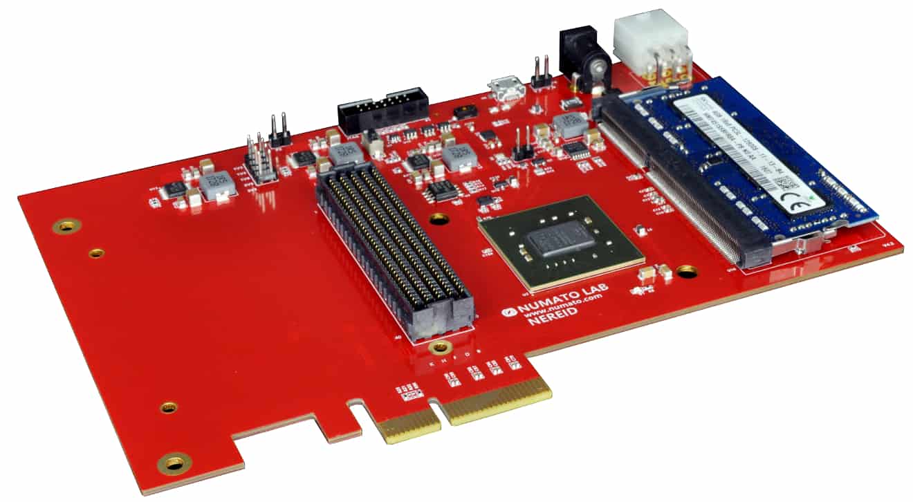
Nereid is an easy to use FPGA Development Board featuring Xilinx Kintex-7 FPGA with x4 PCIe interface and 4GB DDR3L SDRAM. This board features Xilinx XC7K160T– FBG676 FPGA. Other FPGA configurations are available at request. The board features High Pin Count (HPC) high-speed FMC connector conforming to ANSI/VITA 57.1 Standard for the purpose of adding additional features to the board by using custom or commercial off-the-shelf daughter boards.
Applications:
- Parallel Processing and Accelerators
- Product Prototype Development
- Development and Testing of custom embedded processors
- Signal Processing
- Communication Devices Development
- Data Acquisition
- Educational tool for Schools and Universities
Board features
- FPGA: Kintex-7 XC7K160T in -1 FBG676 package (Other devices available at request)
- 4 lane PCIe Gen2.0 (5GT/s)
- 4GB DDR3L SODIMM SDRAM M471B5173CB0-YK0 or compatible
- 128 Mb QSPI flash memory (N25Q128A13ESE40E) for Configuration and optional data storage
- USB to UART serial converter
- 1 x 100MHz CMOS oscillator, 1x 150MHz LVDS oscillator for users
- 1 x 150MHz LVDS oscillator for GTX
- Maximum 174 IOs for user-defined purposes on ANSI/VITA 57.1 Standard compliant FMC HPC connector
- 4x GTX lanes up to 6.6Gbps on ANSI/VITA 57.1 Standard compliant FMC HPC connector
- On-board voltage regulators for single power rail operation
- Can be powered from PCIe slot or from an external power supply
- JTAG header for programming and debugging
- All differential pairs are length matched on the board
- 1 RGB LED for custom use
How to Use Nereid Kintex 7 PCI Express Development Board
Hardware Accessories Required
Along with the board, the following accessories are required for easy and fast installation.
- 12 V DC Power Supply (not needed if the board is inserted into a motherboard)
- A Xilinx Platform Cable USB II compatible JTAG programmer
- USB Male A to Micro B cable (optional)
Connection Diagram
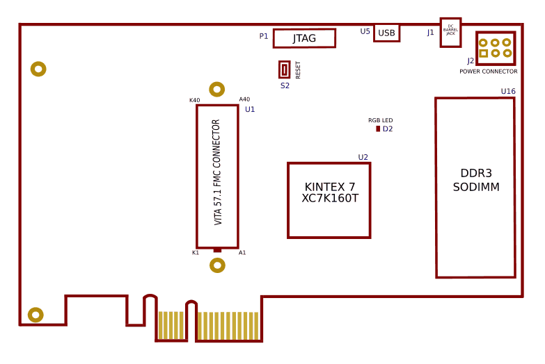
This diagram should be used as a reference only. For detailed information, see Nereid’s schematics and mechanical dimensions at the end of this page. The details of individual connectors are as below.
Power
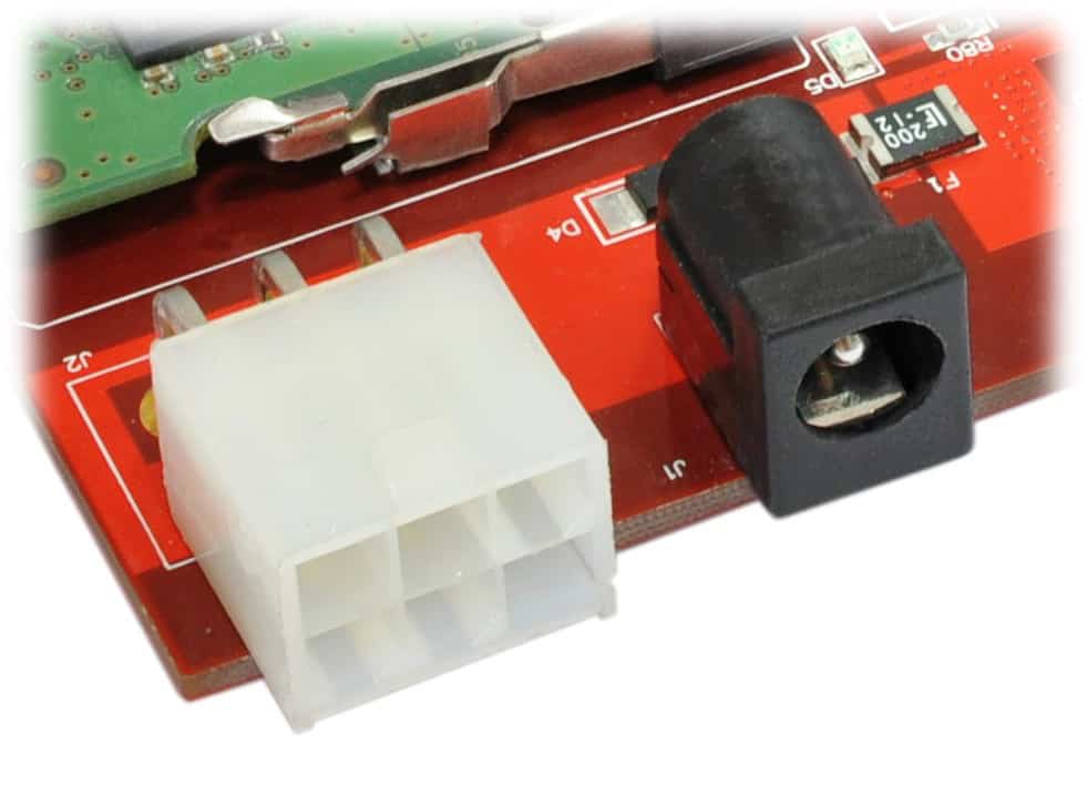 Nereid requires a +12V power supply to function properly. Nereid can be supplied power in 3 ways:
- External +12V power via DC Barrel Jack Connector
- External +12V power via 3×2 PCIe Power Connector.
- Via Motherboard when Nereid is plugged into a PCIe slot that is capable of powering Nereid
The current requirement for this board largely depends on your application. The Nereid module works on a power supply of 1 A of current for simple applications. However, a power supply 2 A of current is recommended for a smooth running of bigger applications. Please consult the FPGA datasheet for more details on power requirements.
USB Serial Bridge
 USB Serial Bridge can be used to interface with PC using the serial interface. It is primarily used to output debug information or as a console for the design running on the board. A Micro USB type cable should be used to connect Nereid to host PC. An FT234 is used as the USB-Serial Bridge IC. The USB-Serial interface features hardware flow control using RTS and CTS signals, in case users need to use hardware flow control. An extra signal CBUS0 from FT234X is also connected to FPGA, which can be used as host-controlled GPIO or can be used for other purposes.
Heat Sink
A Heat Sink (Digikey Part Number: 345-1147-ND) comes factory-installed with Nereid to provide for heat dissipation for the Kintex-7 FPGA onboard. A header is provided to optionally connect a fan (not factory installed) for forced-cooling. The fan’s speed is controlled by the FAN_PWM signal connected to FPGA IO location J25, and the signal is pulled up by default, which means unless actively driven to 0 or controlled via PWM, the fan will run at maximum speed.
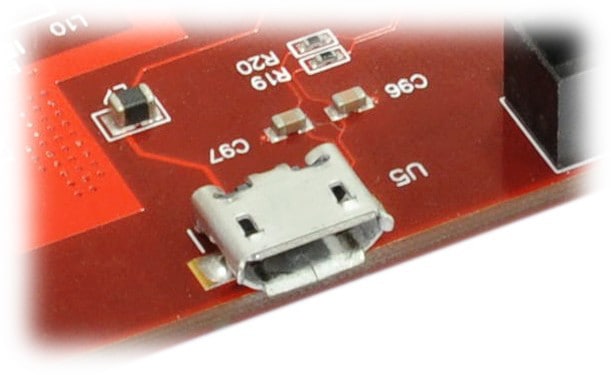
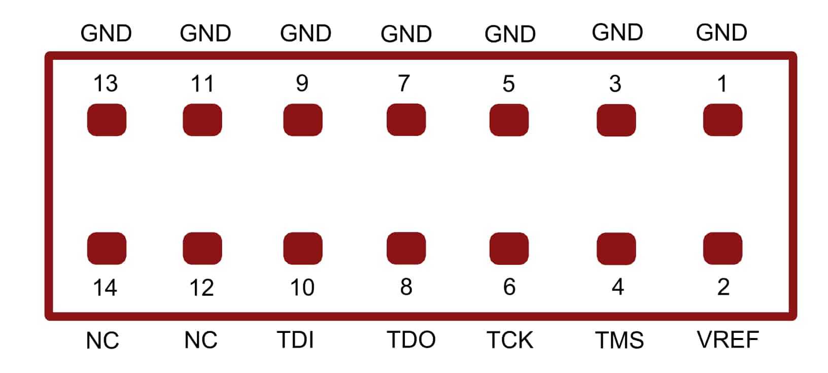
JTAG
JTAG connector allows the FPGA’s JTAG registers to be accessed using a JTAG cable compatible with Xilinx Platform Cable USB. Use this header to attach JTAG cable for programming and debugging.
SODIMM Memory Slot
Nereid features a SODIMM Memory Slot factory-populated with 4GB DDR3L SDRAM. Only compatible modules should be inserted into this slot.
RGB LED
Nereid features one RGB LED which can be used for custom or debug purposes. The LED is wired in the active-low configuration.
JTAG Chain Configuration
JTAG chain can be modified using jumper P2 near JTAG header.
Following diagram shows JTAG chain configuration:
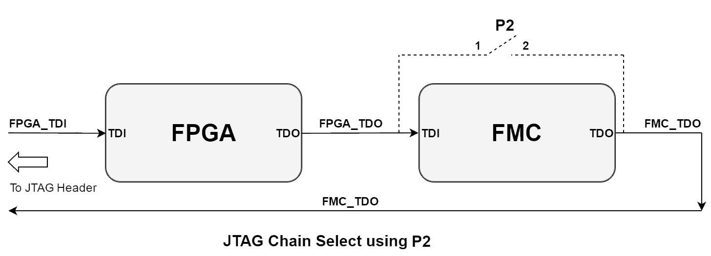
Nereid has automatic FMC detection using the PRSNT_M2C_L signal from FMC. Normally, when an FMC board is not connected, the Nereid’s onboard circuitry will automatically close the JTAG chain keeping FMC out from the chain, so no user intervention is required. But, still, jumper P2 has been provided as a redundant back up to close the JTAG chain in case the automatic circuitry doesn’t work due to non-compliant FMC modules connected to Nereid, or any or unforeseen reasons.
Configuration Mode Switch
FPGA startup configuration mode can be selected using switch S1.
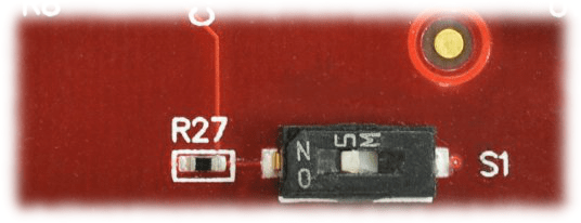
Sliding it to ON puts FPGA in the “JTAG” configuration mode. Sliding it to OFF puts the FPGA to the “Master SPI” configuration mode.
Reset Switch
Nereid features a Push-button S2 normally meant to be used as a “Reset” signal for designs running on FPGA. Push-button S2 is connected to FPGA pin C26. Push-button S2 is active-high, and users need to enable FPGA’s internal Pulldown on the pin C26 to use the pushbutton correctly. This pushbutton can also be used for any other input and is not just limited to be used as a Reset signal.
FMC VADJ Power Supply
VADJ Power Supply for FMC Bank A is configurable via jumpers J3. The following are the jumper configurations for different voltages for the VADJ supply.
| Jumper on J3 Header | FMC VADJ Power Supply (Volts) |
|---|---|
| No jumper anywhere | 3.3 |
| 1 - 2 | 2.5 |
| 3 - 4 | 1.8 |
| 5 - 6 | 1.5 |
| 7 - 8 | 1.2 |
PCIe x4 Edge Connector
PCI Express 2.0 4-lane edge-connector on Nereid can be used to interface with host PCs via PCI Express protocol. Each lane is capable of 5 GT/s resulting in a maximum theoretical data transfer rate of 2 GB/s for all 4 lanes combined.
PCI Express x4 Edge Connector
| Signal Name | Kintex-7 (FBG676) Pin |
|---|---|
| REFCLK_P | K6 |
| REFCLK_N | K5 |
| PCIE_TX0_P | H1 |
| PCIE_TX0_N | H2 |
| PCIE_TX1_P | K1 |
| PCIE_TX1_N | K2 |
| PCIE_TX2_P | M1 |
| PCIE_TX2_N | M2 |
| PCIE_TX3_P | P1 |
| PCIE_TX3_N | P2 |
| PCIE_RX0_P | J3 |
| PCIE_RX0_N | J4 |
| PCIE_RX1_P | L3 |
| PCIE_RX1_N | L4 |
| PCIE_RX2_P | N3 |
| PCIE_RX2_N | N4 |
| PCIE_RX3_P | R3 |
| PCIE_RX3_N | R4 |
| PCIE_PERSTn | E21 |
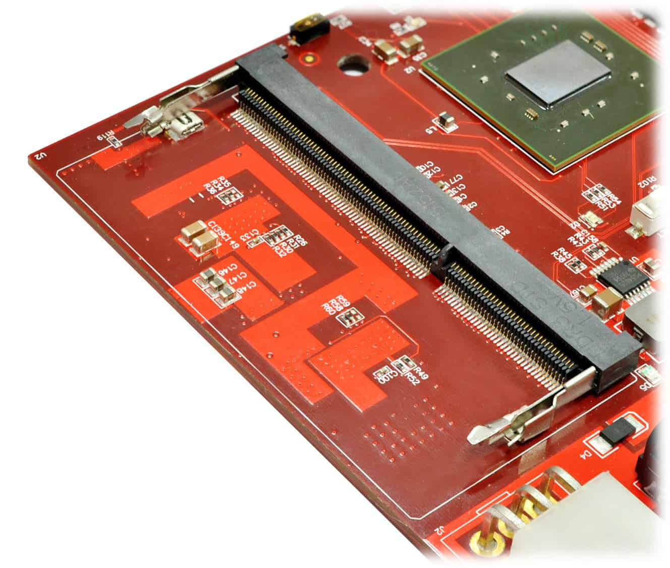
FMC Connector
Nereid features a high speed, high pin-count FMC connector which can be used to provide additional features and capabilities to it using custom or commercial off-the-shelf daughter boards. Apart from IOs, 4 GTX lanes are available via FMC connector for custom purposes.
FMC Banks A to D
| A | FMC Pin Name | Kintex-7 FBG676 Pin | B | FMC Pin Name | Kintex-7 FBG676 Pin | C | FMC Pin Name | Kintex-7 FBG676 Pin | D | FMC Pin Name | Kintex-7 FBG676 Pin |
|---|---|---|---|---|---|---|---|---|---|---|---|
| A1 | GND | GND | B1 | CLK_DIR | D23 | C1 | GND | GND | D1 | PG_C2M | D26 |
| A2 | DP1_M2C_P | E4 | B2 | GND | GND | C2 | DP0_C2M_P | F2 | D2 | GND | GND |
| A3 | DP1_M2C_N | E3 | B3 | GND | GND | C3 | DP0_C2M_N | F1 | D3 | GND | GND |
| A4 | GND | GND | B4 | DP9_M2C_P | NC | C4 | GND | GND | D4 | GBTCLK0_M2C_P | F6 |
| A5 | GND | GND | B5 | DP9_M2C_N | NC | C5 | GND | GND | D5 | GBTCLK0_M2C_N | F5 |
| A6 | DP2_M2C_P | C4 | B6 | GND | GND | C6 | DP0_M2C_P | G4 | D6 | GND | GND |
| A7 | DP2_M2C_N | C3 | B7 | GND | GND | C7 | DP0_M2C_N | G3 | D7 | GND | GND |
| A8 | GND | GND | B8 | DP8_M2C_P | NC | C8 | GND | GND | D8 | LA01_P_CC | Y23 |
| A9 | GND | GND | B9 | DP8_M2C_N | NC | C9 | GND | GND | D9 | LA01_N_CC | AA24 |
| A10 | DP3_M2C_P | B6 | B10 | GND | GND | C10 | LA06_P | Y25 | D10 | GND | GND |
| A11 | DP3_M2C_N | B5 | B11 | GND | GND | C11 | LA06_N | Y26 | D11 | LA05_P | W25 |
| A12 | GND | GND | B12 | DP7_M2C_P | NC | C12 | GND | GND | D12 | LA05_N | W26 |
| A13 | GND | GND | B13 | DP7_M2C_N | NC | C13 | GND | GND | D13 | GND | GND |
| A14 | DP4_M2C_P | NC | B14 | GND | GND | C14 | LA10_P | V21 | D14 | LA09_P | W20 |
| A15 | DP4_M2C_N | NC | B15 | GND | GND | C15 | LA10_N | W21 | D15 | LA09_N | Y21 |
| A16 | GND | GND | B16 | DP6_M2C_P | NC | C16 | GND | GND | D16 | GND | GND |
| A17 | GND | GND | B17 | DP6_M2C_N | NC | C17 | GND | GND | D17 | LA13_P | K20 |
| A18 | DP5_M2C_P | NC | B18 | GND | GND | C18 | LA14_P | J18 | D18 | LA13_N | J20 |
| A19 | DP5_M2C_N | NC | B19 | GND | GND | C19 | LA14_N | J19 | D19 | GND | GND |
| A20 | GND | GND | B20 | GBTCLK1_M2C_P | D6 | C20 | GND | GND | D20 | LA17_P_CC | E18 |
| A21 | GND | GND | B21 | GBTCLK1_M2C_N | D5 | C21 | GND | GND | D21 | LA17_N_CC | D18 |
| A22 | DP1_C2M_P | D2 | B22 | GND | GND | C22 | LA18_P_CC | F17 | D22 | GND | GND |
| A23 | DP1_C2M_N | D1 | B23 | GND | GND | C23 | LA18_N_CC | E17 | D23 | LA23_P | C17 |
| A24 | GND | GND | B24 | DP9_C2M_P | NC | C24 | GND | GND | D24 | LA23_N | C18 |
| A25 | GND | GND | B25 | DP9_C2M_N | NC | C25 | GND | GND | D25 | GND | GND |
| A26 | DP2_C2M_P | B2 | B26 | GND | GND | C26 | LA27_P | G15 | D26 | LA26_P | J15 |
| A27 | DP2_C2M_N | B1 | B27 | GND | GND | C27 | LA27_N | F15 | D27 | LA26_N | J16 |
| A28 | GND | GND | B28 | DP8_C2M_P | NC | C28 | GND | GND | D28 | GND | GND |
| A29 | GND | GND | B29 | DP8_C2M_N | NC | C29 | GND | GND | D29 | TCK | |
| A30 | DP3_C2M_P | A4 | B30 | GND | GND | C30 | SCL | C21 | D30 | TDI | R7 |
| A31 | DP3_C2M_N | A3 | B31 | GND | GND | C31 | SDA | B21 | D31 | TDO | |
| A32 | GND | GND | B32 | DP7_C2M_P | NC | C32 | GND | GND | D32 | 3P3VAUX | VCC3V3 |
| A33 | GND | GND | B33 | DP7_C2M_N | NC | C33 | GND | GND | D33 | TMS | |
| A34 | DP4_C2M_P | NC | B34 | GND | GND | C34 | GA0 | GND | D34 | TRST_L | NC |
| A35 | DP4_C2M_N | NC | B35 | GND | GND | C35 | 12P0V | VCC12V0 | D35 | GAI | GND |
| A36 | GND | GND | B36 | DP6_C2M_P | NC | C36 | GND | GND | D36 | 3P3V | VCC3V3 |
| A37 | GND | GND | B37 | DP6_C2M_N | NC | C37 | 12P0V | VCC12V0 | D37 | GND | GND |
| A38 | DP5_C2M_P | NC | B38 | GND | GND | C38 | GND | GND | D38 | 3P3V | VCC3V3 |
| A39 | DP5_C2M_N | NC | B39 | GND | GND | C39 | 3P3V | VCC3V3 | D39 | GND | GND |
| A40 | GND | GND | B40 | RES0 | NC | C40 | GND | GND | D40 | 3P3V | VCC3V3 |
FMC Banks E to H
| E | FMC Pin Name | Kintex-7 FBG676 Pin | F | FMC Pin Name | Kintex-7 FBG676 Pin | G | FMC Pin Name | Kintex-7 FBG676 Pin | H | FMC Pin Name | Kintex-7 FBG676 Pin |
|---|---|---|---|---|---|---|---|---|---|---|---|
| E1 | GND | GND | F1 | PG_M2C | E26 | G1 | GND | GND | H1 | VREF_A_M2C | NC |
| E2 | HA01_P_CC | N21 | F2 | GND | GND | G2 | CLK1_M2C_P | AC23 | H2 | PRSNT_M2C_L | B26 |
| E3 | HA01_N_CC | N22 | F3 | GND | GND | G3 | CLK1_M2C_N | AC24 | H3 | GND | GND |
| E4 | GND | GND | F4 | HA00_P_CC | P23 | G4 | GND | GND | H4 | CLK0_M2C_P | Y22 |
| E5 | GND | GND | F5 | HA00_N_CC | N23 | G5 | GND | GND | H5 | CLK0_M2C_N | AA22 |
| E6 | HA05_P | R18 | F6 | GND | GND | G6 | LA00_P_CC | AA23 | H6 | GND | GND |
| E7 | HA05_N | P18 | F7 | HA04_P | N19 | G7 | LA00_N_CC | AB24 | H7 | LA02_P | AD26 |
| E8 | GND | GND | F8 | HA04_N | M20 | G8 | GND | GND | H8 | LA02_N | AE26 |
| E9 | HA09_P | N18 | F9 | GND | GND | G9 | LA03_P | AA25 | H9 | GND | GND |
| E10 | HA09_N | M19 | F10 | HA08_P | U19 | G10 | LA03_N | AB25 | H10 | LA04_P | AD25 |
| E11 | GND | GND | F11 | HA08_N | U20 | G11 | GND | GND | H11 | LA04_N | AE25 |
| E12 | HA13_P | U24 | F12 | GND | GND | G12 | LA08_P | U26 | H12 | GND | GND |
| E13 | HA13_N | U25 | F13 | HA12_P | T24 | G13 | LA08_N | V26 | H13 | LA07_P | V23 |
| E14 | GND | GND | F14 | HA12_N | T25 | G14 | GND | GND | H14 | LA07_N | V24 |
| E15 | HA16_P | R25 | F15 | GND | GND | G15 | LA12_P | M17 | H15 | GND | GND |
| E16 | HA16_N | P25 | F16 | HA15_P | P24 | G16 | LA12_N | L18 | H16 | LA11_P | L19 |
| E17 | GND | GND | F17 | HA15_N | N24 | G17 | GND | GND | H17 | LA11_N | L20 |
| E18 | HA20_P | M25 | F18 | GND | GND | G18 | LA16_P | T18 | H18 | GND | GND |
| E19 | HA20_N | L25 | F19 | HA19_P | K25 | G19 | LA16_N | T19 | H19 | LA15_P | U17 |
| E20 | GND | GND | F20 | HA19_N | K26 | G20 | GND | GND | H20 | LA15_N | T17 |
| E21 | HB03_P | J13 | F21 | GND | GND | G21 | LA20_P | K16 | H21 | GND | GND |
| E22 | HB03_N | H13 | F22 | HB02_P | H14 | G22 | LA20_N | K17 | H22 | LA19_P | H16 |
| E23 | GND | GND | F23 | HB02_N | G14 | G23 | GND | GND | H23 | LA19_N | G16 |
| E24 | HB05_P | B15 | F24 | GND | GND | G24 | LA22_P | C19 | H24 | GND | GND |
| E25 | HB05_N | A15 | F25 | HB04_P | B14 | G25 | LA22_N | B19 | H25 | LA21_P | D19 |
| E26 | GND | GND | F26 | HB04_N | A14 | G26 | GND | GND | H26 | LA21_N | D20 |
| E27 | HB09_P | D14 | F27 | GND | GND | G27 | LA25_P | F19 | H27 | GND | GND |
| E28 | HB09_N | D13 | F28 | HB08_P | E13 | G28 | LA25_N | E20 | H28 | LA24_P | D15 |
| E29 | GND | GND | F29 | HB08_N | E12 | G29 | GND | GND | H29 | LA24_N | D16 |
| E30 | HB13_P | B12 | F30 | GND | GND | G30 | LA29_P | E15 | H30 | GND | GND |
| E31 | HB13_N | B11 | F31 | HB12_P | B10 | G31 | LA29_N | E16 | H31 | LA28_P | G17 |
| E32 | GND | GND | F32 | HB12_N | A10 | G32 | GND | GND | H32 | LA28_N | F18 |
| E33 | HB19_P | A9 | F33 | GND | GND | G33 | LA31_P | G19 | H33 | GND | GND |
| E34 | HB19_N | A8 | F34 | HB16_P | D9 | G34 | LA31_N | F20 | H34 | LA30_P | H17 |
| E35 | GND | GND | F35 | HB16_N | D8 | G35 | GND | GND | H35 | LA30_N | H18 |
| E36 | HB21_P | H9 | F36 | GND | GND | G36 | LA33_P | L17 | H36 | GND | GND |
| E37 | HB21_N | H8 | F37 | HB20_P | J11 | G37 | LA33_N | K18 | H37 | LA32_P | H19 |
| E38 | GND | GND | F38 | HB20_N | J10 | G38 | GND | GND | H38 | LA32_N | G20 |
| E39 | VADJ | VCCVADJ | F39 | GND | GND | G39 | VADJ | VCCVADJ | H39 | GND | GND |
| E40 | GND | GND | F40 | VADJ | VCCVADJ | G40 | GND | GND | H40 | VADJ | VCCVADJ |
FMC Banks J to K
| J | FMC Pin Name | Kintex-7 FBG676 Pin | K | FMC Pin Name | Kintex-7 FBG676 Pin |
|---|---|---|---|---|---|
| J1 | GND | GND | K1 | VREF_B_M2C | H11/C13 |
| J2 | CLK3_BIDIR_P | R21 | K2 | GND | GND |
| J3 | CLK3_BIDIR_N | P21 | K3 | GND | GND |
| J4 | GND | GND | K4 | CLK2_BIDIR_P | R22 |
| J5 | GND | GND | K5 | CLK2_BIDIR_N | R23 |
| J6 | HA03_P | AD23 | K6 | GND | GND |
| J7 | HA03_N | AD24 | K7 | HA02_P | AB22 |
| J8 | GND | GND | K8 | HA02_N | AC22 |
| J9 | HA07_P | R16 | K9 | GND | GND |
| J10 | HA07_N | R17 | K10 | HA06_P | P16 |
| J11 | GND | GND | K11 | HA06_N | N17 |
| J12 | HA11_P | P19 | K12 | GND | GND |
| J13 | HA11_N | P20 | K13 | HA10_P | T20 |
| J14 | GND | GND | K14 | HA10_N | R20 |
| J15 | HA14_P | R26 | K15 | GND | GND |
| J16 | HA14_N | P26 | K16 | HA17_P_CC | M21 |
| J17 | GND | GND | K17 | HA17_N_CC | M22 |
| J18 | HA18_P | N26 | K18 | GND | GND |
| J19 | HA18_N | M26 | K19 | HA21_P | M24 |
| J20 | GND | GND | K20 | HA21_N | L24 |
| J21 | HA22_P | T22 | K21 | GND | GND |
| J22 | HA22_N | T23 | K22 | HA23_P | U22 |
| J23 | GND | GND | K23 | HA23_N | V22 |
| J24 | HB01_P | F14 | K24 | GND | GND |
| J25 | HB01_N | F13 | K25 | HB00_P_CC | E10 |
| J26 | GND | GND | K26 | HB00_N_CC | D10 |
| J27 | HB07_P | G10 | K27 | GND | GND |
| J28 | HB07_N | G9 | K28 | HB06_P_CC | C12 |
| J29 | GND | GND | K29 | HB06_N_CC | C11 |
| J30 | HB11_P | A13 | K30 | GND | GND |
| J31 | HB11_N | A12 | K31 | HB10_P | C9 |
| J32 | GND | GND | K32 | HB10_N | B9 |
| J33 | HB15_P | E11 | K33 | GND | GND |
| J34 | HB15_N | D11 | K34 | HB14_P | F9 |
| J35 | GND | GND | K35 | HB14_N | F8 |
| J36 | HB18_P | G12 | K36 | GND | GND |
| J37 | HB18_N | F12 | K37 | HB17_P_CC | G11 |
| J38 | GND | GND | K38 | HB17_N_CC | F10 |
| J39 | VIO_B_M2C | FMC_VIO_B_M2C | K39 | GND | GND |
| J40 | GND | GND | K40 | VIO_B_M2C | FMC_VIO_B_M2C |
USB-Serial Bridge Driver
Installing Driver for USB Serial Converter on Windows
This board requires a driver to be installed to use USB serial converter, for the board’s proper functioning when used with Windows. Ideally, Windows should automatically search and install the correct driver for Nereid via Windows Update. For manual installation, the FTDI VCP drivers are available for download from http://www.ftdichip.com/.
Generating Bitstream Using Vivado
The PCI Express specification requires cards to be ready for link training within 100 ms after the host PC’s power supply is stable.
The following constraints need to be added to the xdc file before synthesizing, implementing and generating a bitstream for a PCI Express design. These can be safely ignored if the PCI Express interface is not used in the design.
set_property BITSTREAM.CONFIG.CONFIGRATE 16 [current_design]
set_property BITSTREAM.GENERAL.COMPRESS TRUE [current_design]
set_property BITSTREAM.CONFIG.SPI_BUSWIDTH 4 [current_design]
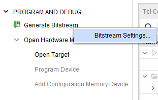
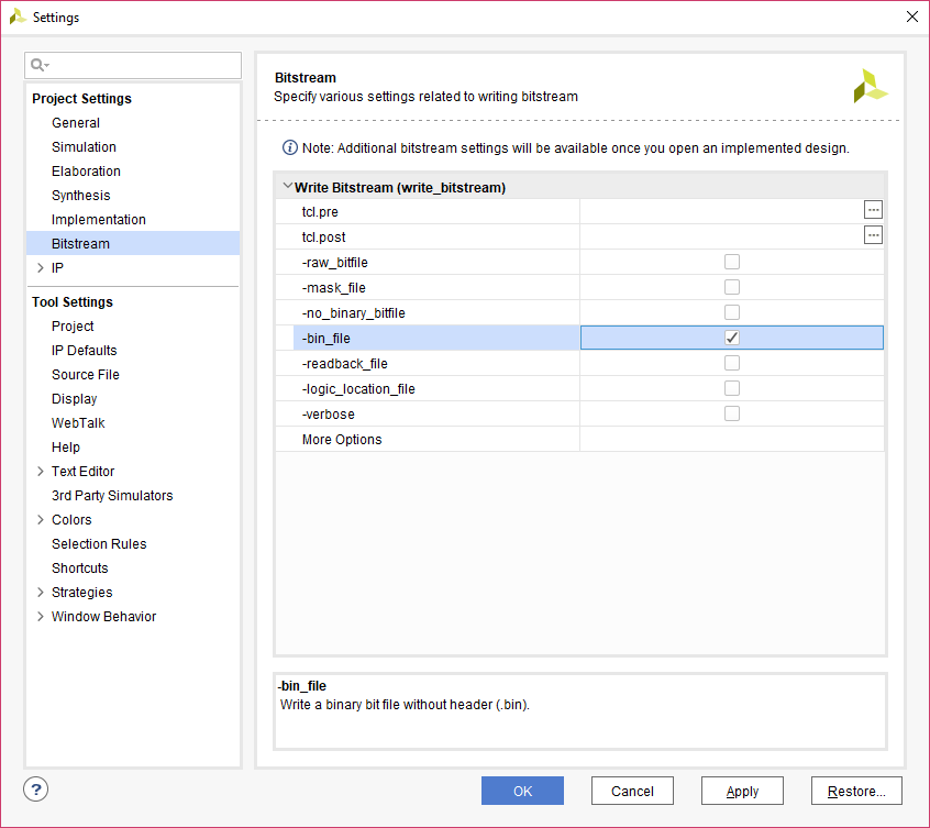
Step 1: It is recommended to generate a .bin bitstream file along with .bit bitstream file. Click “Bitstream Settings”.
Step 2: Select the “-bin_file*” option in the dialog window and click OK.
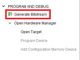
Step 3: Finally click “Generate Bitstream”.
Programming Nereid Using JTAG
Nereid Kintex-7 PCI Express FPGA Board features an onboard JTAG connector that facilitates easy reprogramming of SRAM and onboard SPI flash through JTAG programmer like “Xilinx Platform cable USB”. The following steps illustrate how to program FPGA on Nereid using JTAG.
Step 1: Connect Xilinx Platform cable USB to Nereid using JTAG cable. Power up Nereid.
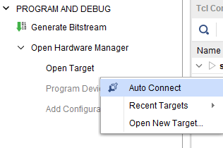
Step 2: Open Vivado Project. Click on “Open Target” in “Open Hardware Manager” in the “Program and Debug” section of the Flow Navigator window. Select “Auto Connect”.
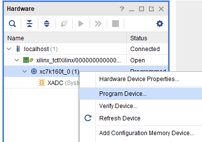
Step 3: If the device is successfully detected, then right-click on the “xc7k160t_0”. Select “Program Device” as shown below.
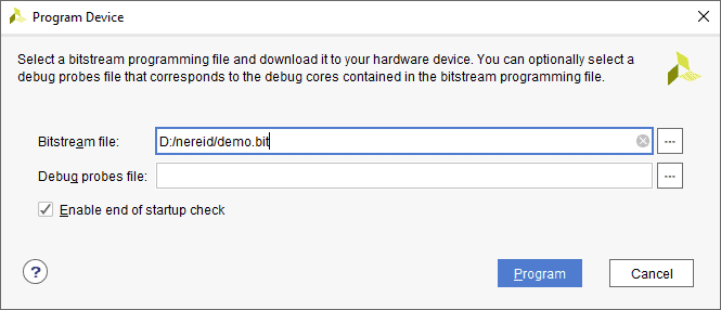
Step 4: In the dialog window which opens up, Vivado automatically chooses the correct bitstream file if the design was synthesized, implemented and bitstream generated successfully. If needed, browse to the bitstream which needs to be programmed to FPGA. Finally click “Program”.
As soon as “Program” is clicked, a green colored LED (D1) on Nereid should light up, indicating that the programming process is going on. This LED will turn off when the configuration is complete.
Programming QSPI Flash using Vivado
A .bin or .mcs file is required for programming Nereid’s onboard QSPI flash.
Step 1: Open Vivado Project. Click on “Open Target” in “Open Hardware Manager” in the “Program and Debug” section of the Flow Navigator window.
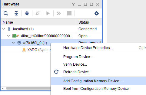
Step 2: If the device is successfully detected, then right-click on the “xc7k160t_0”. Select “Add Configuration Memory Device” as shown below.
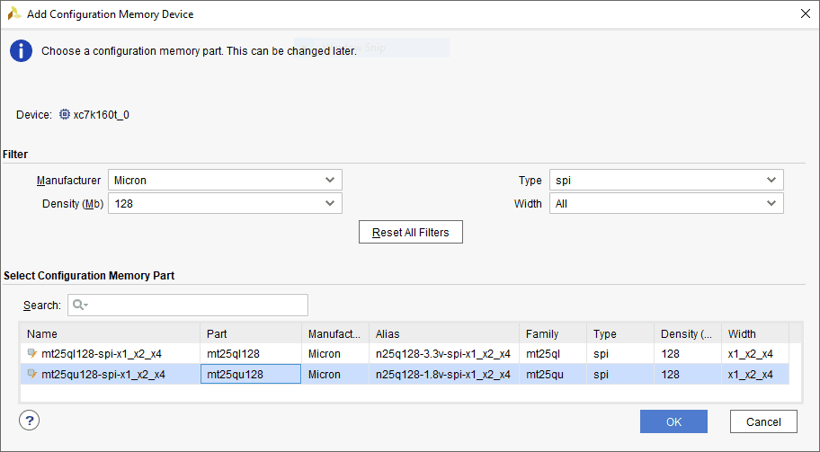
Step 3: Select the memory device “n25q128-3.3v-spi-x1_x2_x4”, then click OK.
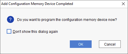
Step 4: After completion of Step 3 the following dialog box will open. Click OK.
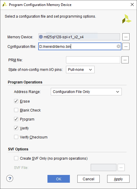
Step 5: Browse to the working .bin file or the .mcs file (whichever applicable) and click OK to program as shown below. If programming is successful, a confirmation message will be displayed.
Technical Specifications
| Parameter * | Value | Unit |
|---|---|---|
| Basic Specifications | ||
| Number of GPIOs (Max) | 174 | |
| On-board Oscillator Frequency (ASEM1- 100.000MHZ-LC-T) | 100 (x1) | MHz |
| On-board Oscillator Frequency (ASVMPLV- 150.000MHZ-L-T)(1 for GTP, 1 for User purpose) | 150 (x2) | MHz |
| DDR3 (M471B5173CB0-YK0) | 4 (x1) | GB |
| SPI Flash Memory (N25Q128A13ESE40E) | 128 | Mb |
| Power supply voltage (External) | 12 | V |
| FPGA Specifications | ||
| Internal supply voltage relative to GND | -0.5 to 1.32 | V |
| Auxiliary supply voltage relative to GND | -0.5 to 3.75 | V |
| Output drivers supply voltage relative to GND | -0.5 to 3.75 | V |
| Connector Header (populated on Nereid) Specifications (0459714515) | ||
| Number of Positions | 400 | |
| Number of Rows | 10 | |
| Height above Board | 8.05 | mm |
| Pitch | 1.27 | mm |
| Mated Stacking Height | 10, 10.5, 11, 11.5, 12.5, 13, 15 | mm |
| Mating Connector for FMC Daughter module | 0459704715 |
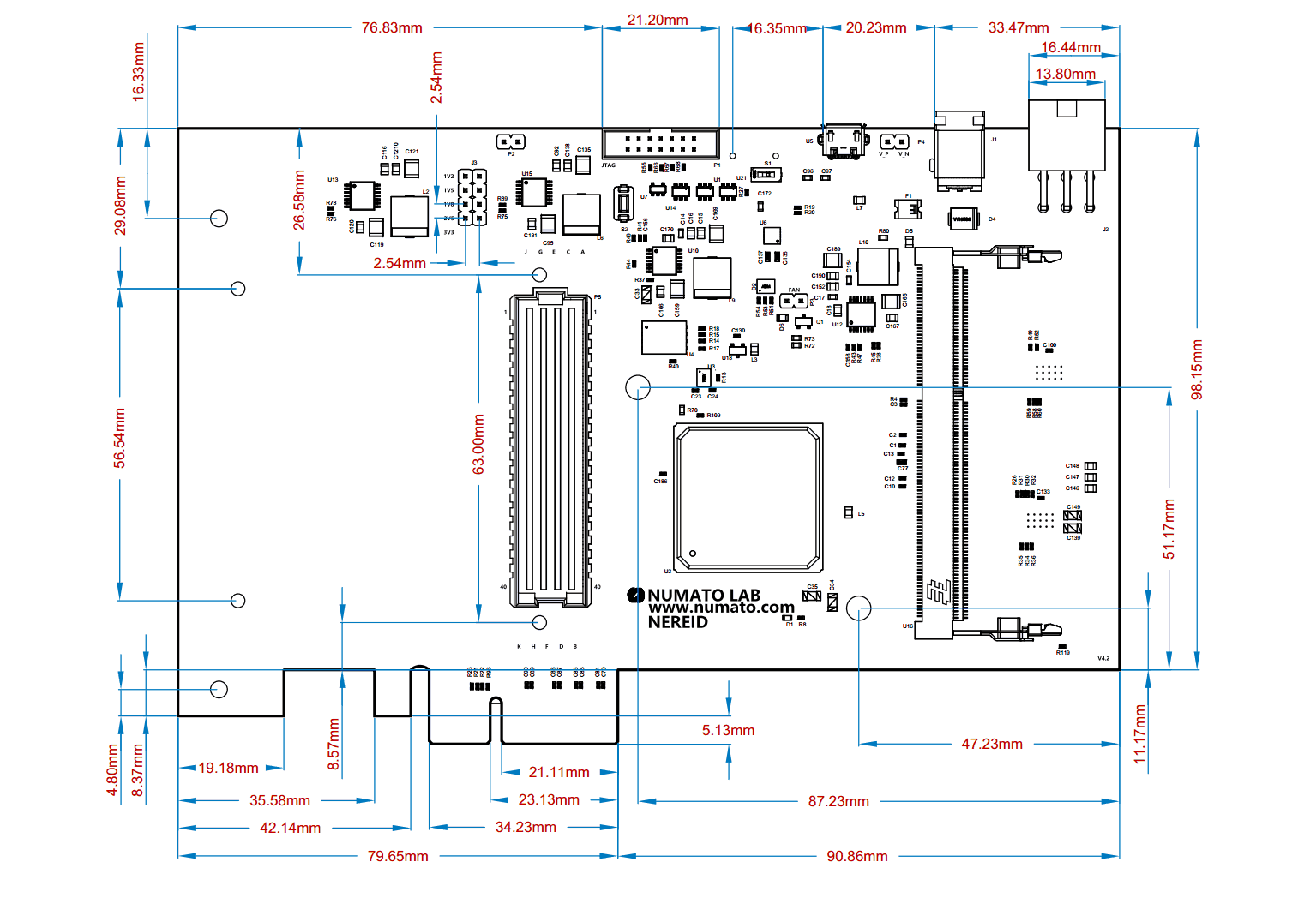
Mechanical Dimensions