Introduction
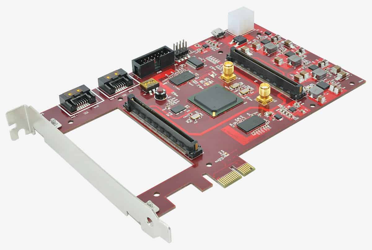
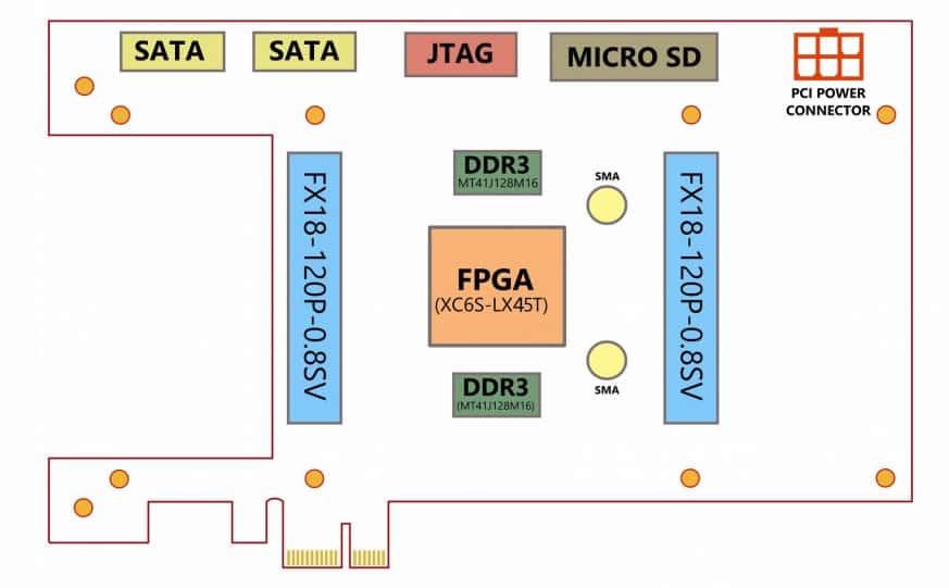
Galatea is an easy to use FPGA Development board featuring Xilinx Spartan-6 FPGA with x1 PCIe interface and two 1Gb DDR3 SDRAM devices. This board features Xilinx XC6SLX45T – FGG484 FPGA. Other FPGA configurations are available at request. Two high-speed expansion connectors are available onboard for the purpose of adding additional features to the board by using custom or off-the-shelf daughter boards. A rich set of off-the-shelf expansion modules are available at http://numato.com.
Applications
- Product Prototype Development
- Development and testing of custom embedded processors
- Signal Processing
- Communication devices development
- Data Acquisition
- Educational tool for Schools and Universities
Board features
- FPGA: Spartan-6 XC6SLX45T in -3FGG484 package (Other devices available at request)
- 1 lane PCIe Gen1 interface • 2 x DDR3: 1Gb SDRAM MT41J128M16
- 128 Mb QSPI flash memory (N25Q128A13ESE40E) for Configuration and optional data storage
- USB to UART serial converter
- 3 x 100MHz CMOS oscillator
- 2 x 150MHz CMOS oscillator for GTP
- 2 x GTP available on 2x SATA connectors
- MicroSD adapter for bulk data storage
- All differential pairs are length matched on the module
- Maximum 112 IOs for user-defined purposes on FX18 Hirose connectors
- On-board voltage regulators for single power rail operation
- Can be powered from PCIe slot or from an external power supply
- JTAG and SPI headers for programming and debugging
- 44 Length matched LVDS33 differential pairs
- 12 Length matched LVDS1V5 differential pairs
- 2x SMA connectors for Clock or other signal input
How to Use Galatea PCI Express Spartan 6 FPGA Development Board
Components/Tools Required
Along with the module, you may need the items in the list below for easy and fast installation.
1. 12 V DC Power Supply (not needed if the board is placed on a motherboard)
2. A Xilinx Platform Cable USB II compatible JTAG programmer
3. USB Male A to Micro B cable (optional)
Connection Diagram
This diagram should be used as a reference only. For detailed information, see Galatea schematics at the end of this document. Details of individual connectors are as below.
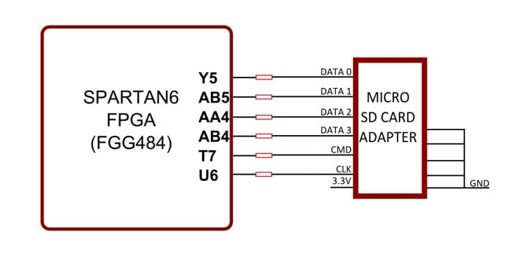
Micro SD
This board features a Micro SD adapter on-board. By installing a Micro SD card and appropriate IP, you can add data logging, media storage and other file storage to your design. The FPGA IOs connected to SD card adapter is shown below.
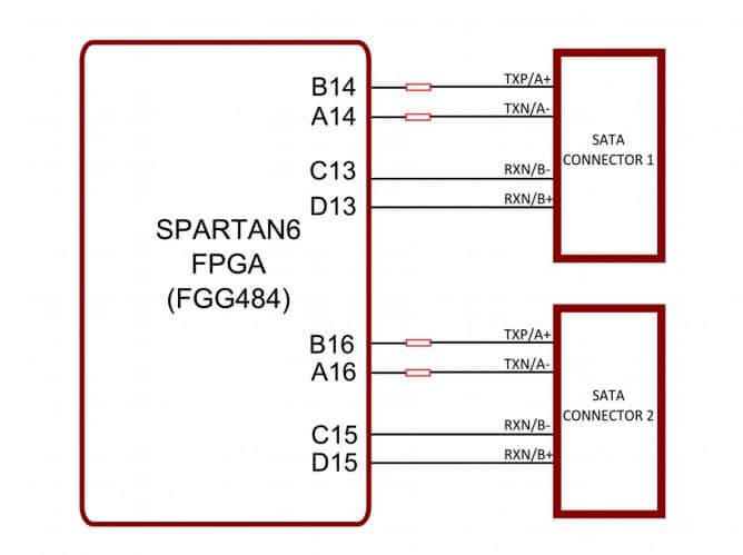
GTP Transceivers on SATA Connectors
Galatea features two SATA connectors onboard which are connected to two of the four available GTP Transceivers on the FPGA. These GTP lines can be used for high-speed communication protocols with appropriate IP. IO details in the image below.
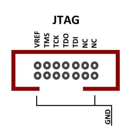
JTAG
JTAG connector allows the FPGA’s JTAG registers to be accessed using a JTAG cable compatible with Xilinx Platform Cable USB. Use this header to attach JTAG cable for programming and debugging.
Connector/Device Pinouts
PCIe Connector
| Pin No. | Pin Name | Spartan-6 (FGG484) Pin No. |
|---|---|---|
| A13 | PCIE_CLK_Q0_P | A10 |
| A14 | PCIE_CLK_Q0_N | B10 |
| A16 | PCIE_TX0_P | B6 |
| A17 | PCIE_TX0_N | A6 |
| A14 | PCIE_RX0_P | D7 |
| A15 | PCIE_RX0_N | C7 |
| A11 | PCIE_PERST_N | F10 |
QSPI (N25Q128A13ESE40E)
| Pin No. | Pin Name | Spartan-6 (FGG484) Pin No. |
|---|---|---|
| 1 | SPI_CS_N | AA3 |
| 2 | SPI_DO_DIN_MISO1 | AA20 |
| 3 | SPI_D1_MISO2 | R13 |
| 5 | SPI_MOSI_CSI_N_MISO0 | AB20 |
| 6 | SPI_CLK | Y20 |
| 7 | SPI_D2_MISO3 | T14 |
SMA
| Pin Name | Spartan-6 (FGG484) Pin No. |
|---|---|
| EXCLK0 | U12 |
| EXCLK1 | T12 |
GPIOs
This device is equipped with a maximum of 112 user GPIO pins that can be used for custom applications. All differential pairs are length matched on the module for better signal integrity.
Header P4
| Header Pin No. | Spartan-6 (FGG484) Pin No. | Pin Description | Header Pin No. | Spartan-6 (FGG484) Pin No. | Pin Description |
|---|---|---|---|---|---|
| 1 | - | GND | 17 | J17 | IO_L19N_1 |
| 2 | C11 | MGTREFCLK1P_101 | 18 | - | GND |
| 3 | D11 | MGTREFCLK1N_101 | 19 | H16 | IO_L9P_1 |
| 4 | - | GND | 20 | H17 | IO_L9N_1 |
| 5 | D9 | IMGTRXP1_101 | 21 | - | GND |
| 6 | C9 | MGTRXN1_101 | 22 | B21 | IO_L10P_1 |
| 7 | - | GND | 23 | B22 | IO_L10N_1 |
| 8 | B8 | MGTTXP1_101 | 24 | - | GND |
| 9 | A8 | MGTTXN1_101 | 25 | J7 | IO_L81P_3 |
| 10 | - | GND | 26 | H8 | IO_L81N_3 |
| 11 | TMS | 27 | - | GND | |
| 12 | TCK | 28 | H12 | IO_L35P_GCLK17_0 | |
| 13 | TDO | 29 | G11 | IO_L35N_GCLK16_0 |
|
| 14 | TDO | 30 | - | GND | |
| 15 | - | GND | 31 | H10 | IO_L33P_0 |
| 16 | J16 | IO_L19P_1 | 32 | H11 | IO_L33N_0 |
| 33 | - | GND | 63 | G4 | IO_L58N_3 |
| 34 | G8 | IO_L32P_0 | 64 | - | GND |
| 35 | F9 | IO_L32N_0 | 65 | F3 | IO_L60P_3 |
| 36 | - | GND | 66 | E4 | IO_L60N_3 |
| 37 | C5 | IO_L32N_0 | 67 | - | GND |
| 38 | A5 | IO_L8N_VREF_0 | 68 | D2 | IO_L59P_3 |
| 39 | - | GND | 69 | D1 | IO_L59N_3 |
| 40 | H13 | IO_L38P_0 | 70 | - | GND |
| 41 | G13 | IO_L38N_VREF_0 | 71 | H6 | IO_L80P_3 |
| 42 | - | GND | 72 | G7 | IO_L80N_3 |
| 43 | F7 | IO_L7P_0 | 73 | - | GND |
| 44 | F8 | IO_L7N_0 | 74 | F14 | IO_L36P_GCLK15_0 |
| 45 | - | GND | 75 | F15 | IO_L36N_GCLK14_0 |
| 46 | D4 | IO_L2P_0 | 76 | - | GND |
| 47 | D5 | IO_L2N_0 | 77 | H14 | IO_L49P_0 |
| 48 | - | GND | 78 | G15 | IO_L49N_0 |
| 49 | B2 | IO_L3P_0 | 79 | - | GND |
| 50 | A2 | IO_L3N_0 | 80 | E5 | IO_L4P_0 |
| 51 | - | GND | 81 | E6 | IO_L4N_0 |
| 52 | B3 | IO_L5P_0 | 82 | - | GND |
| 53 | A3 | IO_L5N_0 | 83 | E16 | IO_L37P_GCLK13_0 |
| 54 | - | GND | 84 | F16 | IO_L37N_GCLK12_0 |
| 55 | C4 | IO_L6P_0 | 85 | - | GND |
| 56 | A4 | IO_L6N_0 | 86 | C17 | IO_L50P_0 |
| 57 | - | GND | 87 | A17 | IO_L50N_0 |
| 58 | C3 | IO_L1P_HSWAPEN_0 | 88 | - | GND |
| 59 | D3 | IO_L1N_VREF_0 | 89 | G16 | IO_L51P_0 |
| 60 | - | GND | 90 | F17 | IO_L51N_0 |
| 61 | - | GND | 91 | - | GND |
| 62 | H4 | IO_L58P_3 | 92 | D18 | IO_L62P_0 |
| 93 | D19 | IO_L62N_VREF_0 | 107 | - | GND |
| 94 | - | GND | 108 | - | GND |
| 95 | B18 | IO_L63P_SCP7_0 | 109 | - | GND |
| 96 | A18 | IO_L63N_SCP6_0 | 110 | - | 5V |
| 97 | - | GND | 111 | - | 5V |
| 98 | C19 | IO_L64P_SCP5_0 | 112 | - | GND |
| 99 | A19 | IO_L64N_SCP4_0 | 113 | - | 12V |
| 100 | - | GND | 114 | - | 12V |
| 101 | B20 | IO_L65P_SCP3_0 | 115 | - | GND |
| 102 | A20 | IO_L65N_SCP2_0 | 116 | - | 1V2 |
| 103 | - | GND | 117 | - | 1V2 |
| 104 | D17 | IO_L66P_SCP1_0 | 118 | - | 3V3 |
| 105 | C18 | IO_L66N_SCP0_0 | 119 | - | 3V3 |
| 106 | - | GND | 120 | - | GND |
Header P5
| Header Pin No. | Spartan-6 (FGG484) Pin No. | Pin Description | Header Pin No. | Spartan-6 (FGG484) Pin No. | Pin Description |
|---|---|---|---|---|---|
| 1 | - | GND | 13 | - | TDO |
| 2 | - | NC | 14 | - | TDO |
| 3 | - | NC | 15 | - | GND |
| 4 | - | GND | 16 | AA2 | IO_L10P_3 |
| 5 | - | NC | 17 | AA1 | IO_L10N_3 |
| 6 | - | NC | 18 | - | GND |
| 7 | - | GND | 19 | U4 | IO_L24P_3 |
| 8 | - | NC | 20 | T4 | IO_L24N_3 |
| 9 | - | NC | 21 | - | GND |
| 10 | - | GND | 22 | W4 | IO_L2P_3 |
| 11 | - | TMS | 23 | Y3 | IO_L2N_3 |
| 12 | - | TCK | 24 | - | GND |
| 25 | P5 | IO_L9P_3 | 55 | Y16 | IO_L17P_2 |
| 26 | P4 | IO_L9N_3 | 56 | W15 | IO_L17N_2 |
| 27 | - | GND | 57 | - | GND |
| 28 | AA12 | IO_L31P_GCLK31_D14_2 | 58 | W17 | IO_L5P_2 |
| 29 | AB12 | IO_L31N_GCLK30_D15_2 | 59 | Y18 | IO_L5N_2 |
| 30 | - | GND | 60 | - | GND |
| 31 | W10 | IO_L44P_2 | 61 | - | GND |
| 32 | Y10 | IO_L44N_2 | 62 | V5 | IO_L8P_3 |
| 33 | - | GND | 63 | V3 | IO_L8N_3 |
| 34 | AA10 | IO_L41P_2 | 64 | - | GND |
| 35 | AB10 | IO_L41N_VREF_2 | 65 | P6 | IO_L25P_3 |
| 36 | - | GND | 66 | P7 | IO_L25N_3 |
| 37 | W9 | IO_L48P_D7_2 | 67 | - | GND |
| 38 | Y8 | IO_L48N_RDWR_B_VREF_2 | 68 | N6 | IO_L23P_3 |
| 39 | - | GND | 69 | N7 | IO_L23N_3 |
| 40 | V13 | IO_L18P_2 | 70 | - | GND |
| 41 | W13 | IO_L18N_2 | 71 | T6 | IO_L7P_3 |
| 42 | - | GND | 72 | T5 | IO_L7N_3 |
| 43 | T10 | IO_L46P_2 | 73 | - | GND |
| 44 | U10 | IO_L46N_2 | 74 | R11 | IO_L22P_2 |
| 45 | - | GND | 75 | T11 | IO_L22N_2 |
| 46 | Y15 | IO_L21P_2 | 76 | - | GND |
| 47 | AB15 | IO_L21N_2 | 77 | T15 | IO_L23P_2 |
| 48 | - | GND | 78 | U15 | IO_L23N_2 |
| 49 | U16 | IO_L4P_2 | 79 | - | GND |
| 50 | V15 | IO_L4N_VREF_2 | 80 | W14 | IO_L20P_2 |
| 51 | - | GND | 81 | Y14 | IO_L20N_2 |
| 52 | AA16 | IO_L19P_2 | 82 | - | GND |
| 53 | AB16 | IO_L19N_2 | 83 | Y11 | IO_L32P_GCLK29_2 |
| 54 | - | GND | 84 | AB11 | IO_L32N_GCLK28_2 |
| 85 | - | GND | 103 | - | GND |
| 86 | U9 | IO_L50P_2 | 104 | W6 | IO_L60P_2 |
| 87 | V9 | IO_L50N_2 | 105 | Y6 | IO_L60N_2 |
| 88 | - | GND | 106 | - | GND |
| 89 | T8 | IO_L57P_2 | 107 | - | GND |
| 90 | U8 | IO_L57N_2 | 108 | - | GND |
| 91 | - | GND | 109 | - | GND |
| 92 | AA8 | IO_L45P_2 | 110 | - | 5V |
| 93 | AB8 | IO_L45N_2 | 111 | - | 5V |
| 94 | - | GND | 112 | - | GND |
| 95 | Y7 | IO_L47P_2 | 113 | - | 12V |
| 96 | AB7 | IO_L47N_2 | 114 | - | 12V |
| 97 | - | GND | 115 | - | GND |
| 98 | V7 | IO_L58P_2 | 116 | - | NC |
| 99 | W8 | IO_L58N_2 | 117 | - | NC |
| 100 | - | GND | 118 | - | 3V3 |
| 101 | R9 | IO_L59P_2 | 119 | - | 3V3 |
| 102 | R8 | IO_L59N_2 | 120 | - | GND |
Configuring Galatea Using JTAG
Galatea Spartan 6 FPGA Board features an onboard JTAG connector that facilitates easy reprogramming of SRAM and onboard SPI flash through JTAG programmer like “Xilinx Platform cable USB”. Programming Galatea using JTAG requires “Xilinx ISE iMPACT” software which is bundled with Xilinx ISE Design Suite. The FPGA SRAM can be programmed using the .bit file generated from your project. To program the SPI flash we need to generate a “.mcs” file which must be generated from the “.bit” file. Steps for generating the “.mcs” file are as below. Programming FPGA SRAM does not require a “.mcs” file to be generated.
Generating “.mcs” file for Galatea
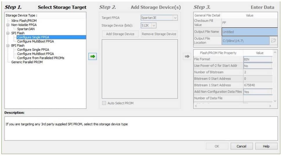
Step 1: Open ISE iMPACT. Click on “Create PROM file(PROM file formatter)”. In the dialog box, select “Configure Single FPGA” in the storage device type. Then click on the green arrow on the right side.
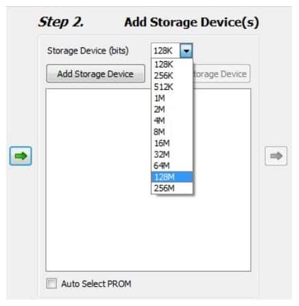
Step 2: Select 128M in Storage Device (bits). Now click on “Add Storage Device”, then the green arrow on the right side.
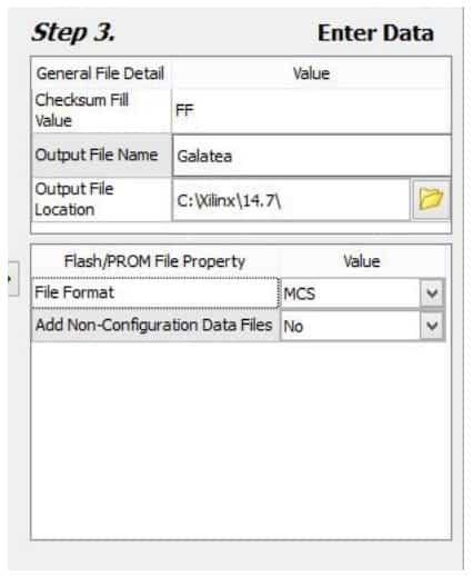
Step 3: Set an output file name and the output file location (a “.mcs” extension will be generated at this location and the file will be required later for programming the FPGA), then click OK twice, then select the “.bit” file we already generated then click Open and click NO when it prompts to add another device file.
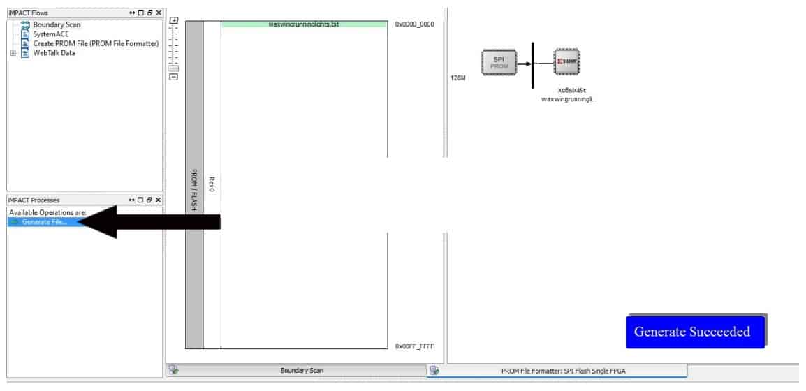
Step 4: Double click on the “Generate File” option under the iMPACT processes window. “Generate Succeeded” message will be displayed as shown in the image below if the “.mcs” the file is generated successfully.
Programming SPI Flash Using ISE iMPACT
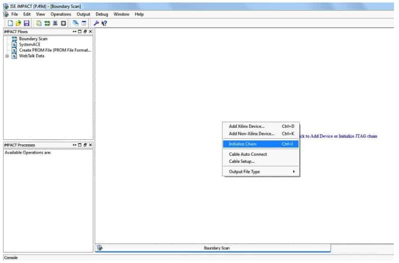
Step 1: Open ISE iMPACT. Click on “Boundary Scan” in the iMPACT flows window on the left top corner. Then right-click on the window panel on the right. Select “Initialize Chain”.
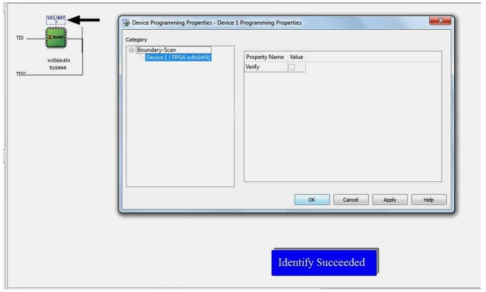
Step 2: If the device is detected properly you will see a pop-up window as shown below, Click OK. Then right-click on the SPI/BPI (next to the black arrow in the below fig.), select Add SPI/BPI Flash.
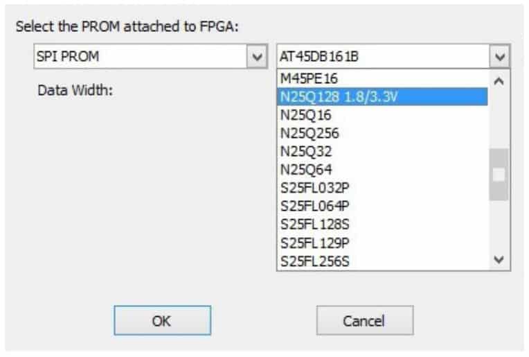
Step 3: Select the “.mcs” file we already created and click OK. Now choose “N25Q128” in the dialogue box that appears, then click OK.
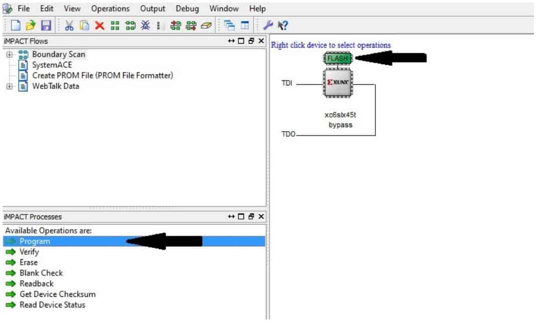
Step 4: Click on “Flash” and then double click on Program option in iMPACT processes window. If programming is successful, a confirmation message will be displayed.
Technical Specifications
| Parameter * | Value | Unit |
|---|---|---|
| Basic Specifications | ||
| Number of GPIOs (Max) | 112 | |
| On-board oscillator frequency (FXO-HC536R) | 100 (x 3) | MHz |
| DDR3: | 1 (x2) | Gb |
| SPI Flash Memory (N25Q128A13ESE40E) | 128 | Mb |
| Power supply voltage (External) | 12 | V |
| FPGA Specifications | ||
| Internal supply voltage relative to GND | –0.5 to 1.32 | V |
| Auxiliary supply voltage relative to GND | –0.5 to 3.75 | V |
| Output drivers supply voltage relative to GND | –0.5 to 3.75 | V |
| Connector Header Specifications (FX18-120P-0.8SV) | ||
| Number of Positions | 120 | |
| Number of Rows | 2 | |
| Pitch | 0.80 | mm |
| Height | 8.65 | mm |
| Mated, Stacking Heights | 15, 20 | mm |
| Current Rating(Max.) | 3 | Amp |
| Mating Receptacles | FX18-120S-0.8SV15 FX18-120S-0.8SV20 FX18-120S-0.8SH |
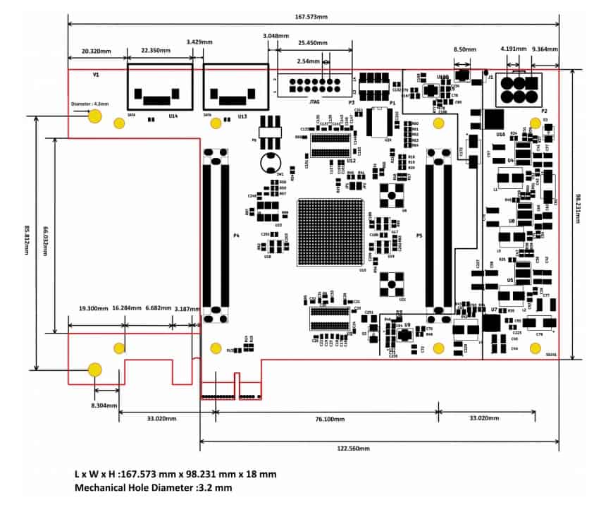
Mechanical Dimension